
Kuang Sheng
College of Electrical Engineering, Zhejiang University, Hangzhou, 310027, China
Abstract
With superior material properties, wide bandgap power semiconductor devices (SiC and GaN) can offer performances orders-of-magnitude better than their silicon counterparts. As a result, they are widely expected to be the next generation power devices. In this paper, developments and current status of wide bandgap power semiconductor devices including SiC and GaN will be reviewed. Remaining challenges and trends for future developments will be discussed.
1. Introduction
For more than half a century, the continuous evolution of power semiconductor devices has enabled tremendous developments of the power electronic technologies The development of power semiconductor devices have predominately been based on silicon material, namely, the foundation of the general semiconductor industry. Nevertheless, starting from as early as late 1980s, it has been recognized that basic physical properties of silicon material is imposing a limit on the performance of power devices. Such a limit is best represented by the equation below for unipolar devices of a given semiconductor material, ![]() where
where  is the device specific onresistance,
 is the breakdown voltage,
 is the material permittivity,
 is the carrier mobility and
  is the material critical electrical field. Equation (1) indicates that the device on resistance for a given chip size is proportional to the square of its breakdown voltage and hence increases quickly as its breakdown voltage increases. This is due to the fact that both the thickness and resistivity of the active voltage blocking layer in the device need to be increased roughly proportionally in order for the device to block a higher voltage. Resistances of unipolar devices such as MOSFETs and JFETs become excessive for devices blocking 600V or higher voltages and bipolar devices offering conductivity modulation become necessary. As a result, Si IGBT has been a hugely successful example that is currently dominating the medium voltage and medium-to-high power applications. Nevertheless, charge injection and extraction times re-lated to the conductivity modulation make the dynamic performances of these bipolar devices significantly inferior to those of the unipolar counterparts, hence limiting their high frequency applications. It is worth noting that the introduction of super-junction concept [1,2] made it possible to achieve resistances lower than what is stated in equation (1) and such technologies have been commercialized. Nevertheless, obtaining resistances much lower than the limit in equation (1) requires extreme semiconductor processing abilities that are currently difficult to obtain.
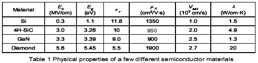
It is clear from equation (1) that the best way of achieving a low device specific on-resistance is to increase the material critical electric field which is closely related to the bandgap of a semiconductor device. Table 1 shows the band-gap, critical electric field and other important physical properties of a few semiconductor mate-rials. It can be seen that the critical field of the three wide bandgap semiconductor materials are at least one order of magnitude higher than that of the silicon. Substituting the physical parameters into equation (1), is can be concluded that the specific on-resistances SiC, GaN and diamond unipolar devices are about 600, 700 and 4300 times lower than that of the silicon unipolar device, respectively. This is the factor of conduction loss reduction if the same chip size is used for all devices based on different materials.
A more realistic estimation [3] considering both the device conduction loss, switching loss and chip size selection reveals that the total device losses can be reduced by a factor of 7.5, 8.0 and 23.8 for SiC, GaN and diamond, respectively. The corresponding chip-size reduction factors are 65 times, 62 times and 220 times for SiC, GaN and diamond, respectively. Such loss andchip-size reductions are drastic and can lead torevolutionary changes in power electronics systems.
In addition to the lower device losses and chipsizes, the higher electron saturation velocities ofthe three listed wide bandgap materials alsomake them superior on high frequency RF applications. The high thermal conductivities of SiC and diamond materials make them ideal for highpower applications where significant amount ofheat needs to be dissipated and the materialthermal impedance contributes significantly to the overall system thermal impedance.
Due to their attractive performances, wide bandgap power semiconductor devices have been under intense research and development efforts. Since the foundations of these attractive per-formances come from the materials themselves, the first challenge to take in research is the preparation of high quality semiconductor materials that can be used for the fabrication of power semiconductor devices.
2. Silicon Carbide Power De-vices
Out of the three wide bandgap materials listedabove, the development of SiC material for power device application has gone through the longest period and come furthest in terms of maturity and reliability. Since early 1990s, a significant amount of effort has been invested in obtaining high quality single crystalline SiC substrate and epitaxial materials. In 2004, high quality 3” 4H-SiC materials with micropipe density lower than 10cm-2have been made commercially available by Cree Inc. In 2007, the same company started to offer 4” zero-micropipe 4H-SiC materials that can be used to fabricate large-size high power devices. These 4” wafers are now at full production at Cree and in final qualification phase at II‐VI, Dow Corning and Nippon Steel. 6” wafers have already been announced by 2010. 150 mm wafers will definitely accelerate the cost reduction of SiC device manufacturing and provide a solid foundation for the development of 4H-SiC power devices.
2.1. SiC power diodes
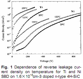
There are three types of SiC power diodes, namely the Schottky Barrier Diode (SBD), the P-i-N diode and the Junction Barrier Schottky diode (JBS). With a Schottky barrier, the SBD usually has a relatively low junction barrier height. As aresult, the SBD has the advantage of a low turn-on voltage (ranging from 0.7V to 1.5V, depending on the Schottky metal used and device processing details) in its forward conduction mode. However, using a metal with a lower forward turn-on voltage usually leads to a higher reverse leakage current. Fig. 1 [4] shows the reverse leakage cur-rents of two SBDs with different metals. It is noted that the leakage current increases quickly with the reverse bias due to a so-called “image-force-lower” effect on the Schottky barrier height. On the other hand, a P-i-N diode could have a very low and stable reverse leakage current. Nevertheless, due to its structure, it has a high forward turn-on voltage of approximately 2.7V at room temperature, which limits its application to voltages higher than ~5kV.
The third choice, namely, the JBS diode attemps to combine the benefits of both the SBD and the P-i-N diode by integrating the two structure together [5]. This structure features a low turn-on voltage like that of the SBD but has a reverse leakage current similar to the P-i-N diode. This advantage makes the JBS structure the preferred choice for devices at medium voltages or below.
Diodes with very high breakdown voltages have also been reported in SiC. A SBD with a breakdown voltage of 10.8kV and a specific onresistance of 97mcm2 has been reported in [6] and a P-i-N diode with a breakdown voltage of 19kV has been reported in [7].
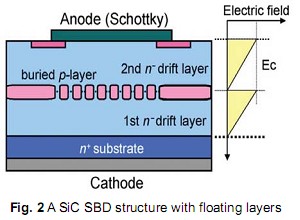
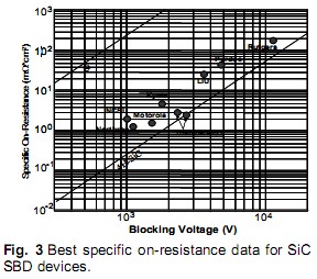
There have also been continued improvements on the diode specific on-resistance of SiC SBDs. In Fig. 2, a SiC SBD structure with floating layers is plotted [8]. The floating layer structure is known to offer similar advantages to those of a super-junction structure yet are less challenging to fabricate. With this structure, it is possible to obtain uniploar devices with specific onresistances lower than those predicted by equation (1). A specific on-resistance as low as was report at a breakdown voltage of 2700V. The best SiC SBD specific on-resistance results have been plotted in Fig. 3. It is clear that the performances of SiC SBDs are approaching the theoretical limit offered by the SiC material. 4.5kV SiC P-i-N diode with an on-state voltage of 3.2V at 180A (100A/cm2) has been reported by Cree in [9]. Apart from the P-i-N diodes, much of the research and development efforts have hence been directed towards improving the manufacturability, reliability, current rating and yield of the SiC SBD and JBS devices.
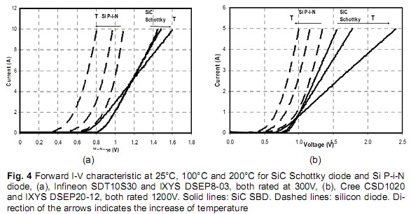
Since 2001, SiC SBDs (JBS devices) have been commercially available. Currently, SiC diodes with voltage ratings of 300V, 600V and 1200V are commercially available from both Infineon Technology and Cree Inc. Single-chip current ratings as high as 50A are also available. In Fig. 4, the forward I-V curves of SiC SBDs and Si P-i-N diodes are compared [5]. A major difference between these two types of devices is the temperature coefficient of the I-V curves. Due to its unipolar nature, the SiC diodes have a predominately positive temperature coefficient, making it easier for connecting multiple chips in parallel for a high current module. This is especially true for the 1200V rated devices. It is worth noting that the plotted 1200V SiC is rated at 5A and the corresponding Si P-i-N diode is rated at 30A.
As unipolar devices, the unique advantage of the SiC diodes is that there is no bipolar storage in the diode during forward conduction. As a result, its reverse recovery charge only comprises the junction depletion charge, which is virtually zero as compared to the recovery charge of a comparable Si diode.
2.2. SiC power BJTs
SiC power BJT is an attractive candidate for SiC power switching appliations. Due to its superior material property, it does not suffer from the secondary breakdown problem that limited the application of Si power BJTs. When compared to the other two SiC power switching devices (JFETs or MOSFETs), it does not suffer from the normally-on or gate driving issues of the SiC JFET devices, nor does not have the complication of a MOS oxide interface and its reliability and/or channel mobility issue. It also has the advantage of relatively easy to fabricate.
Currently, there are two main issues with the SiC BJT. Firstly, as a current driving device, it has a disadvantage of requiring a continuous base driving current when remaining at on-state. Therefore, its current gain has to be sufficiently high to avoid significant driving power drain and a complicated base driving circuitry. Currently, room temperature current gains of SiC BJTs are commonly reported at a level of around 20~30, which could drop below 20 when the device junction heats up. In order to drive the device into saturation, a significant amount of base current and power is needed [10]. Secondly, there have been reports on degradation of SiC BJT current gain and on-resistances after the device is operated [11]. Such degradation was believed to be caused by bulk recombination in the device due to the generation and growth of stacking faults (Basal Plane Defects). The energy released during the recombination of minority carriers in this bipolar device leads to the growth of the stacking faults, which leads to reduced current path and increased on-resistance. This mechanism was not observed in unipolar devices where significant minority carrier recombination does not occur.
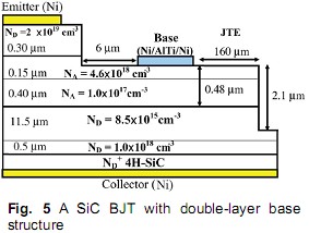
There have been attempts in addressing the issue of low current gain by using graded base doping [12] or double layer base doping [13], as shown in Fig. 5. Both approaches aims at minimizing or avoiding the additional base ohmic contact implantation that can further damage the etched base surface, increase surface recombination and reduce current gain. Current gains exceeding 100 have been reported [13, 14]. Nevertheless, devices with such high current gains are not commonly available. Another approach of solving the current gain problem is to connect two BJTs in a darlington connection. Effective current gain higher than 1500 has been reported in [15]. Nevertheless, in a SiC BJT darlington connection, the main BJT never goes into saturation and the combined collector I-V curve has a knee voltage of 2.7V before any current can pass through the darlington device. Such a high on-state voltage makes this connection only attractive at voltages higher than 5 to 10kV, where it will have to compete against SiC IGBT.
At the same time, a lot of efforts have been invested in solving the second issue raised above, namely, the degradation issue, by improving the epitaxial growth technique. With good material growth condition, basal plane defects can be minimized and the resultant degradation can be largely avoided [13].
SiC BJTs with a breakdown voltage of 9.3kV have been reported and its specific on-resistances have been approaching the theoretical SiC unipolar limit at high blocking voltages. It is worth noting that due to its low minority carrier lifetime, SiC BJTs available today have limited carrier storage and conductivity modulation effects. It has been reported that switching behaviour of SiC BJTs does not show observable storage time and hence can be as fast as unipolar devices [16] with switching times in the order of 10~30ns.
Currently, SiC BJT samples are commercially available from TranSiC Corp. at 1200V with current ratings of 6A and 20A. Due to its superior material property, some of these devices can be housed in high temperature packages and the device can operate at as hot as 250C.
2.3. SiC power JFETs
SiC power JFET is another important candidate for power switching applications. As a unipolar voltage controlled device, it avoids the two issues explained in the previous subsection associated with the BJT. In addition, as it does not have the gate oxide in its structure, it also does not suffer from the complication and reliability concerns surrounding the MOS oxide. It fabrication is also relatively easy.
The only major issue facing SiC power JFETs is that it is often fabricated as a normally-on (or depletion mode) device. Without an active negative gate bias, the device remains at on-state. Such behaviour makes device protection complicated in case of gate driving circuit failure such as the loss of gate driver circuit power supply and hence can be problematic. There are two methods that can be used to address the above issue partially or fully.
The first method is to design a JFET channel sufficiently narrow and/or long so that even when the gate bias is zero, the self depletion of the gate junction stops the drain current from going through the device. Designing and fabrication these “normally-off” power JFETs have been proven to be possible [17] and 1.7kV devices with a specific on-resistance as low as ![]() have been reported. Semisouth Inc. has also adopted a similar approach in obtaining SiC power JFETs that can withstand a good amount of voltage with its gate-to-source voltage is maintained at 0V.
have been reported. Semisouth Inc. has also adopted a similar approach in obtaining SiC power JFETs that can withstand a good amount of voltage with its gate-to-source voltage is maintained at 0V.
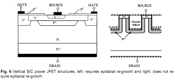
Fig. 6 [18] shows two SiC power JFET structures that can be used to obtain a normally-off feature. One of them requires an epi re-growth and the other does not. Currently, epi re-growth is a technology not widely used and hence is lacking certain maturity. On the other hand, the one that does not require an epi re-growth has the following issues. In order to obtain relatively uniform gate threshold voltages with good control, it requires that the mesa-width and JFET channel opening be controlled with deep sub-micron ac-curacy, making the processing and control of the deep anisotropic etching challenging. Considering the processing tolerances, normally-off SiC power JFETs suffer from a significantly higher on-resistance resulted from a long and narrow JFET channel. Furthermore, the gate of a SiC JFET is usually biased at below 2.7V at on-state to avoid significant gate driving current. With a positive threshold voltage, the room left to overdrive the gate to obtain low device resistance is minimal, seriously limiting the JFET static and dynamic performances.
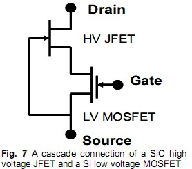
This leads to the second method of solving the SiC JFET threshold voltage issue, namely, the cascode connection. Fig. 7 shows a cascade connection of a SiC high voltage JFET and a Si low voltage MOSFET. The high voltage SiC JFET typically has a threshold voltage of -20~-10V and the low voltage MOSFET is capable of blocking ~30V with a standard power MOSFET threshold voltage. The combined pair has a gate driving characteristics of the standard power MOSFETand the current/voltage capability of the high voltage SiC JFET. In addition, due to i), the de-coupling of the SiC JFET gate and the MOSFET gate and ii), the minimal JFET gate-to-source capacitance, miller effect during switching transients has been largely eliminated. This leads to a rapid switching action whereby the switching times are limited only by the load current and circuit layout parasitics [19].
Due to its normally-on nature, SiC JFETs more suited than other device in acting as current limiting devices[20, 21].
SiC JFET with a blocking voltage as high as11kV and a specific on-resistance of  has been reported [22]. At 700V, a researchteam has achieved the lowest specific on-resistance of
  ever reported for SiC devices [23] by using buried gate structure and by addition substrate processing. Commercial SiC JFET devices are available from Semisouth at 1200V and
  and from SiCED at voltage from 800V to 1800V and resistances as low as
  .
.
2.4. SiC power MOSFETs
Due to its perfect gate impedance, fast switching speed, excellent stability and a relatively low on-state resistance, power MOSFETs have been proven as the device-of-choice in silicon for the voltage range below 300V. As a result, it is generally believed that SiC MOSFET will be the most promising candidate for power electronics applications in the range below3kV to 5kV. The majority of research and development efforts in the SiC power switching field have since been invested on SiC MOSFETs.
However, the developments of SiC power MOSFETs have been hampered by the issues of channel mobility and gate oxide reliability. Both issues stem from a gate oxide whose quality significantly poorer as compared to that of a Si counterpart. The oxidation of SiC in oxygen was proven to be much more problematic than in SiC due to the presence of carbon atoms. As a result, thermally grown oxide layers on SiC have a large amount of interface states that act as traps for the electrons in the channel underneath. Electron mobility in thermally grown SiC MOS channel can be as low as below 10cm2/Vs. This is much lower than that in Si and increases the total device resistance significantly, severely limiting the ability of realizing the potential SiC MOSFET devices. Furthermore, these interface states and traps could lead to device performance instability [24] as well as contributing to long term reliability issues [25].
In recent years, a couple of methods have been proposed to address the issue of the oxide interface. The first is to anneal the gate oxide in a nitrogen environment after it is thermally grown. The proposed methods include NO annealing as well as N2O annealing [26, 27]. It has been revealed that the subsequent annealing decreases the MOS interface states greatly and, as a result, the MOS channel electron mobility has been increased significantly. The increase in channel mobility has led to the successful development of a 1200V SiC MOSFET with a specific onresistance of  [28], making its performance competitive again the other two types of SiC power switches. The second method is to utilize a different crystal face
 ![]() in form-ing the gate oxide [29]. The third method is to grow the gate oxide in a sodium-rich environment. Channel mobilities as high as 200cm2/Vs have been reported. This method is not widely used due to the uncertain nature regarding its device stability.
in form-ing the gate oxide [29]. The third method is to grow the gate oxide in a sodium-rich environment. Channel mobilities as high as 200cm2/Vs have been reported. This method is not widely used due to the uncertain nature regarding its device stability.
With a typical DMOSFET structure, the P-body of the MOSFET has to be implanted. It is also understood that oxide growth on the surface of an implanted P-body is more challenging than that on an epi surface. This leads to additional difficulty in achieving SiC power MOSFET devices with very low specific on-resistances.
Nevertheless, significant achievements have been obtained in developing SiC MOSFET with competitive performance as well as voltage and current handling capabilities. Cree Inc. has reported 8.1mm*8.1mm, 10kV, 20A single Si CMOSFET chips that can be parallel-connected to obtain a high power module capable of conducting 100A [30].
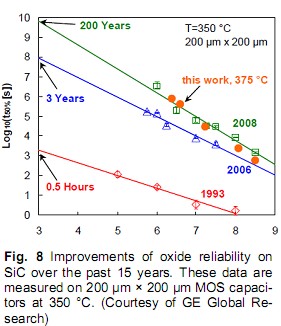
On the other hand, no common consensus regarding the impact of the oxide interface states on its long term reliability has been established throughout the years. Some have expressed concern on the fundamental limit of SiC MOS oxide reliability based on its different band offset structure as compared to its silicon counterpart[31], particularly at higher temperatures. While more recently, oxide reliability measurements have revealed sufficient SiC MOS oxide reliability at temperatures as high as 350C [32]. As shown in Fig. 8, a clear improvement of the SiC MOS oxide reliability in the past two decades has been demonstrated. The recent results make it hopeful that oxide reliability may not ultimately become an issue for SiC MOSFET devices.
The leading parties in this field such as Cree, GE and Infineon are able to produce preliminary samples rated at 1200V, 10~20A. It is expected that SiC MOSFETs rated at 1200V will be commercialized in the next few years time.
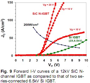
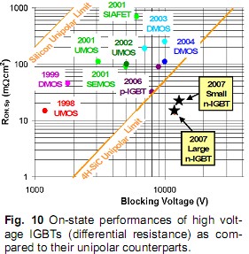
For higher operating voltages such as those higher than 5~10kV, even SiC devices will require a drift layer is that is thick enough to call for conductivity modulation in spite of the additional 2.7V forward voltage drop. As a power device with full control, IGBT has been recognized as the bipolar device-of-choice in Si. Nevertheless, the development of SiC IGBT at higher voltage has been facing two challenges. The first is the same as the MOSFET, namely, the low MOS channel mobility limits the device channel resistance. The second is that an N-channel IGBT requires a P+ substrate which normally comes with a resistivity approximately 50 times higher than its N+ substrate. As a result, to avoid the large substrate resistance, P-channel IGBTs were fabricated first. The first SiC IGBT was fabricated in 1999 and reported in [33]. A 12kV P channel IGBT was recently reported in [34] with good forward current carrying capability. A 12kV N-channel was also reported in 2007 with excellent forward conduction properties [35], as plotted in Fig. 9. The on-state resistances of these IGBT (differential resistances) were compared to those of the unipolar SiC device in Fig. 10 [35]. Differential resistances lower than the theoretical unipolar limit clearly indicates the effect of conductivity modulation.
3. Gallium Nitride Power Devices
Due to the lack of high quality intrinsic substrate, GaN materials are usually grown on other substrates such as SiC, Sapphire or Si. Due to its minimal crystal mismatch, GaN grown on SiC substrates has the best material quality and
hence has been used widely as the choice for high power RF applications. Because of the high cost of SiC substrate, GaN on SiC has not bee able to attract wide attention in the power switching device field. In recent years, significant improvements on the technique of growing GaN material on (111) silicon substrates have enabled high quality, crack-free GaN epi layers grown on Si, overcoming the 17% crystal mismatch between the two materials crystal faces [37]. Because of its huge implication on cost reduction as compared to the SiC technology, this has attracted a tremendous amount of attention in the power switching device field and there have since been reports of various GaN power switching device on Si substrates [38, 39]. Various research groups have worked extensively on improving the epi film uniformity and reducing its defect levels.
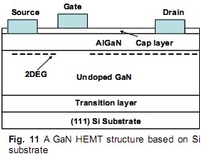
The main advantage of GaN device comes from it wide bandgap property coupled with a unique two Dimensional Electron Gas (2DEG) layer phenomena based on its AlGaN/GaN heterojunction structure. Such a GaN HEMT structure is shown in Fig. 11. Electrons in the 2DEG layer has a sheet density at the order of  and mobility higher than 1200cm2/Vs, significantly higher than similar electron mobility on a SiC surface. This provides an excellent foundation for power devices with low specific on-resistances.
3.1. GaN diodes
GaN diodes can also effectively utilize the 2DEG effect by depositing Pt onto the AlGaN surface to form a Schottky contact [40]. The ohmic contact of the cathode can be form by a combination of Ti/Al/Ti/Au metal layers. Such GaN Schottky diode on Si have been shown to block more than 1kV. GaN diodes with a blocking voltage as high as 9.7kV have been reported on Sapphire substrates [41]. It is expected that the development of GaN Schottky diode will be closely coupled with that of the GaN HEMT as a power switching device in its voltage and current ratings.
3.2. GaN HEMT
Due to the attractive properties of the 2DEG,GaN HEMTs have achieved impressive performances as RF power device as well as for powerswitching applications. A GaN HEMT with a breakdown voltage of 1.3kV and a specific onresistance of 1.7mcm-2 has been reported in [42]. This performance surpasses that of the best SiC power device reported to date and is approximately 1000 times better than the silicon unipolar limit. More recently, GaN devices capable of conducting >5A and blocking >600V have been reported with a specific on-resistance of [43]. Larger devices capable of >70Aand 500V have also been reported [44].
There are two issues facing the development of GaN HEMT. The first is the device threshold voltage that tends to be negative, creating a problem similar to the one explained for SiC JFET in the previous section. A few different approaches have been adopted in increasing the device threshold to an appropriate positive value. One of them uses a low-density drain region by introducing negatively charged fluorine ions which changes the local field distribution and increases the device threshold voltage [45]. Others use a hybrid HEMT/MOS structure [44].
The other major issue the GaN HEMTs have to address before it can be considered for commercial power switching applications is its stability and reliability issues. Due to the nature of its hetero-junction material growth, states and traps are introduced at various material interfaces, including those between the transition layer and the GaN Layer, the AlGaN layer and the top capping layer, etc. To a certain extend, these issues are similar to the SiC MOS interface problem that has been under intense investigation for the past years. Engineering and perfecting these interfaces will be necessary to make reliable GaN high voltage HEMT commercially available.
On the other hand, International Rectifier has recently announced commercially available GaN on Silicon power devices with integrated drivers for low-voltage (<20V) power management applications, highlighting the promises of this technology for power electronics applications at lower power levels.
4. Summary
In this paper, developments and current status of wide bandgap power semiconductor devices including SiC and GaN have been reviewed. A significant amount of achievements have been obtain on the developments of both SiC and GaN devices for power electronics applications. The SiC diode technology is relatively mature for the voltage rage between 600 to 1200V. While there are still some issues with regard to the technologies for SiC three-terminal transistors, SiC samples on all three types of transistors (BJT, JFET and MOSFET) have all been announced and some are already offering preliminary products. It is expected that SiC transistors will start to penetrate the power device market in the near future. It has been estimated [46] that SiC power device market will reach $150 and $800 Million in 2015 and 2019, respectively. The bulk of the market will gradually shift from the low-voltage (<1.2kV) market section to the medium voltage (1.2~1.7kV) section.
At the same time, GaN diodes and HEMT hold great promise in the lower voltage end of the spectrum due to the great potential of GaN-on-Silicon technology in drastically reducing the cost while still maintaining the superior performances of wide bandgap semiconductor devices.
5. Literature
[1] Chen, XB.; US-Patent 5,216,275, 1993
[2] Deboy, G. et al., “A new generation of high voltage MOSFETs breaks the limit line of silicon“, International Electron Devices Meeting, 1998, pp. 683 - 685
[3] Huang, A.Q.; “New unipolar switching power device figures of merit“, IEEE Electron Device Letters, Volume: 25 , No. 5, 2004, pp. 298 - 301
[4] K.P. Schoen, et al., “Design considerations and experimental analysis of high-voltage SiC Schottky barrier rectifiers” Electron Devices, IEEE Trans., 45, 1998, pp. 1595 – 1604
[5] J.H. Zhao, K. Sheng et al., “Silicon Carbide Schottky Barrier Diode“, SiC Materials and Devices – Vol.1, pp 117-162
[6] J.H. Zhao, et al., “Demonstration of the first 10-kV 4H-SiC Schottky barrier diodes” Electron Device Letters, IEEE, 24, 2003, pp. 402-404
[7] Y. Sugawara, et al., "12–19 KV 4H-SiC p-i-n diodes with low power loss,” Proc. Int. Symp. Power Semicond. Dev. ICs (Institute of Electrical Engineers of Japan, Tokyo, 2001), pp. 27–30.
[8] J. Nishio, et al., "Ultralow-Loss SiC Floating Junction Schottky Barrier Diodes (Super-SBDs) " IEEE Trans. Electron Devices, VOL. 55, NO.8, pp.I954-I960, 2008
[9] Hull, B.A., et al., “A 180 Amp/4.5 kV 4H-SiC PiN diode for high current power modules“, Proc. Int. Symp. Power Devices and ICs, ISPSD’2006, pp. 277–280
[10] Ahmed, M.M.R. et al., “Characterization of the static and dynamic behavior of a SiC BJT“, 13th Power Electronics and Motion Control Conference, 2008. EPE-PEMC 2008, pp. 2472 - 2477
[11] A. Agarwal, et al., “Degradation of current gain in SiC. BJTs,” in Proc. Mater. Res. Soc. Symp., 2006, vol. 911, pp. 431–436.
[12] J. H. Zhao, J. Zhang, X. Li, and K. Sheng, “Effect of graded base doping on the gain of SiC BJT,” in Proc. IEEE ISDRS, 2005, pp. 398–399.
[13] J. Zhang, et al., “Implantation-Free 4H-SiC Bipolar Junction Transistors With Double Base Epilayers”, IEEE Electron Device Letters, Vol. 29, No. 5, 2008, pp. 471-473
[14] Q. Zhang, et al., “4H–SiC BJTs with current gain of 110”, Solid-State Electronics Volume 52, Issue 7, July 2008, pp. 1008-1010
[15] J. Zhang, et al., “A 500 V, very high current gain (β = 1517) 4H-SiC bipolar Darlington transistor,” Mater. Sci. Forum, vol. 457–460, pp. 1165–1168, 2004
[16] K. Sheng, et al., ‘High Temperature Characterization of SiC BJTs for Power Switching Applications’, International Journal of Solid-State Electronics, Volume 50, No. 6, 2006, pp. 1073-1079
[17] J. H. Zhao, et al., “3.6 mΩcm2, 1726V 4H-SiC normally-off trenched-and-implanted vertical JFETs”, Proceedings of 15th International Symposium on Power Semiconductor Devices and IC’s (ISPSD), 2003, pp. 50 – 53
[18] J.H. Zhao, K. Sheng, et al., “Current Status andFuture Prospects of SiC Power JFETs and ICs”,IEICE Transaction on Electronics, Vol. E91-C, No7, 2008, pp. 1031-1041
[19] McNutt, T.; et al., “Silicon carbide JFET cascodeswitch for power conditioning applications“, IEEE Conference on Vehicle Power and Propulsion,2005, pp. 499 – 506
[20] Nallet, F., et al., “Electrical and electrothermal 2Dsimulation of a 4H-SiC high voltage current limiting device for serial protection application“.Proc. Int. Symp. Power Devices and ICs,ISPSD’2000, pp. 287–290
[21] Tournier, D., et al., “A 4H-SiC High-power-density VJFET as controlled current limiter“, IEEE Trans. Ind. Appl., 2003, 39, pp. 1508–1513
[22] J. H. Zhao, et al., “Fabrication and Characterization of 11kV Normally off 4H-SiC Trenched-and-Implanted Vertical Junction FET“, IEEE Electron Device Letters,20014,25(7), pp 474-476.
[23] Y. Tanaka, et al., "700V, 1.0mcm2 Buried Gate SiC-SIT (SiC-BGSIT)," IEEE Electron Device Lett., Vol. 27, pp. 908-910, 2006.
[24] A.J. Lelis, et al., “Time Dependence of Bias-Stress-Induced SiC MOSFET Threshold-Voltage Instability Measurements“, IEEE Transactions On Electron Devices, Vol. 55, No. 8, 2008, pp. 1835 -1840
[25] L. Yu, K.P. Cheung, J.S. Suehle, J.P. Campbell, K. Sheng, et al., “Channel Hot-Carrier Effect of 4H-SiC MOSFET”, Material Science Forum, Vols. 615-617, 2009, pp 813-816
[26] H.F. Li, et al., “Effect of NO annealing conditions on electrical characteristics of n-type 4H-SiC MOS capacitors“, Journal of Electronic Materials, Volume 29, Number 8, 2000, pp. 1027-1032
[27] K. Fujihira, et al., “Successful Enhancement of Lifetime for SiO2 on 4H-SiC by N2O Anneal“, IEEE Electron Device Letters, Vol. 25, No. 11, 2004, pp. 734-736
[28] Miura, N., et al., “Successful development of 1.2 kV 4H-SiC MOSFETs with very low on-resistance of 5 mΩcm2“, Proc. Int. Symp. Power Devices and ICs, ISPSD’2006, pp. 261–264
[29] Senzaki, J., et al.,“Significant improvement of inversion channel mobility in 4H-SiC MOSFET on (1120) face using hydrogen post-oxidation annealing“, Mat. Sci. Forum, 2002, 389–393, pp. 1061–1064
[30] John Palmour, “Advances in SiC Power Technology“, 2007
[31] R. Singh and A.R. Hefner, “Reliability of SiC MOS devices“, International Journal of Solid-State Electronics, Vol. 48, 2004, pp. 1717-1720
[32] L. Yu, “Simulation, Modeling And Characterization Of SiC Devices“, Rutgers University, Thesis collection, 2010
[33] Singh, R.; et al., “High temperature, high current, p-channel UMOS 4H-SiC IGBT“, 57th Annual Device Research Conference Digest, 1999, pp. 46 - 47
[34] Q. Zhang, et al., “12-kV p-Channel IGBTs With Low On-Resistance in 4H-SiC“, IEEE Electron Device Letters, Vol. 29, No. 9, 2008
[35] M.K. Das, et al., “ A 13 kV 4H-SiC n-Channel IGBT with Low Rdiff,on and Fast Switching“, Materials Science Forum, Vol. 600 – 603, pp. 1183-1186
[36] A. K. Agarwal, et al., “ A 1cm × 1cm, 5kV, 100A, 4H-SiC Thyristor Chip for High Current Modules“,Materials Science Forum, Vol. 527 - 529, 2006, pp. 1397-1400
[37] J. D. Brown, et al., “AlGaN/GaN HFETs fabricated on 100-mm GaN on silicon (111) substrates”, International journal of Solid-State Electronics, Vol. 46, Issue 10, 2002, pp. 1535-1539
[38] Ueda, D.; et al., “Present and future prospects of gan-based power electronics”, International Conference on Solid-State and Integrated-Circuit Technology, ICSICT 2008, pp. 1078 - 1081
[39] K.S. Im, et al., “Normally-off Operation of Recess-Gated GaN MOSFET on Silicon Sub-strate Using AlGaN/GaN Source/Drain with High 2DEG Density”, ISDRS’09, pp. 1-2
[40] Kamada, A.; et al., “High-Voltage AlGaN/GaN Schottky Barrier Diodes on Si Substrate with Low-Temperature GaN Cap Layer for Edge Termination“, ISPSD’08, pp. 225-228
[41] Zhang, A.P., et al., ‘Lateral AlxGa1-xN powerrectifiers with 9.7 kV reverse breakdown voltage’, Appl. Phys. Lett., 2001, 78, pp. 823–825
[42] N.Q. Zhang, et al., “Effects of Surfance Traps on Breakdown Voltage and Switching Speed of GaN Power Switching HEMTs“, IEDM Tech Dig; 2001. p. 25.5.1–4
[43] X.B. Xin, et. al., „Demonstration of Low-Leakage-Current Low-On-Resistance 600-V 5.5-A GaN/AlGaN HEMT“, IEEE Electron Device Letters, Vol. 30, No. 10, 2009, pp. 1027-1029
[44] H. Kambayashi, et. al., “Enhancement-Mode GaN Hybrid MOS-HFETs on Si Substrates with Over 70 a Operation“, ISPSD’09, pp. 21-24
[45] Y. Cai, et al., “Control of threshold voltage of AlGaN/GaN HEMTs by fluoride-based plasma treatment: From depletion mode to enhancement mode,” IEEE Trans. Electron Devices, vol. 53, no. 9, pp. 2207–2215, Sep. 2006
[46] Yole Developpement, “SiC 2010 Report“, 2010