
Wonseok Kang1, Dongwook Kim2, Sungmo Young2, Taeyoung Ahn3, Seonggi Chang1
1Security R&D Lab., Security Input Device Group, LG Electronics, Korea
wonseok.kang@lge.com
2Application Engineering, HV PCIA, Fairchild Semiconductor, Korea
dongwook.kim@fairchildsemi.com
3Dept. of Electronics Eng., Cheongju University, Korea
Abstract
LLC resonant topology has been used for high frequency power conversion, and now it is very popular for high power density and low profile DC-DC applications. To reduce its output current ripple and power loss further, an interleaving technique is implemented. Because this topology utilizes body diode of a power MOSFET to achieve ZVS condition, it is known that a fast recovery MOSFET is very effective for reliability. In this paper, a new fast recovery MOSFET is introduced. This new device has best-in-class specific on-resistance among available fast recovery body diode MOSFETs, and offers greatly improved power conversion efficiency.
1. Introduction
A LLC resonant converter has many advantages over PWM topologies like ZVS capability for the entire load range, low turn off current, and ZCS operation of the secondary rectifiers.[1] Since there is a discontinuous current flow in secondary rectifiers, a drawback of the LLC resonant converter for high power applications is the ripple current and power losses in capacitors. The interleaving technique is introduced to parallel converters to reduce the ripple current.[2-5] This configuration is very popular along with the extended use of digital controllers. Besides, a fast recovery feature of the body diode is beneficial to the reliability of the LLC resonant converter. It provides improved reliability without any other complex circuitry during power-up or shorted output conditions.[6-7] In terms of power conversion efficiency, the most critical parameter for power switches is on-resistance because switching losses are nearly negligible with the LLC resonant converter. Consequently, an optimum power switch for interleaved LLC resonant converter should have both a fast body diode and the lowest possible on-resistance. A new deep trench epi-filled Super-Junction technology combined with a lifetime control process sets a new benchmark for fast recovery types of high voltage power MOSFETs
2. Interleaved LLC Resonant Converter
Paralleling two or more converters requires phase-shifted control signals. Several publications discussed solutions.[2-5] One possible way is using a toggle flip-flop and inverting logic [5], but it has to do frequency doubling for the transformerhas to do frequency doubling for the transformer design.

Fig. 1. Block diagram of the interleaved LLC converter
An easier way is utilizing a timing signal from resonant converter controller.[3] The controller has triangular timing signal, and therefore its frequency is same as that of a gate driving signal. By using high frequency comparator, it is possible to generate 90º phase-shifted signals. Then, the output of the comparator is fed to FAN73832 HVIC. Figure 1 shows schematic diagram of designed interleaved LLC resonant converter. Figure 2 shows gate drive signals for two paralleled converters and output current at full load. The signals show exact 90º phase-shift as designed.

Fig. 2. Gate driving signals
3. Deep Trench Epi-Filled Technology
Conduction losses can be reduced through realizing the lowest possible on-resistance. In high voltage MOSFET technologies, the most remarkable achievement for on-resistance reduction was a charge-balance technology. This technology has deep P-type pillar-like structure in the body in contrast to well-like structure of conventional planar technology. The effect of the pillars is to confine the electric field in the lightly doped epi region. Due to this P-type pillar, the resistance of N-type epi can be reduced dramatically while maintaining same level of breakdown voltage. Most commercially available Super- Junction devices adopted multiple epi-layers to build the deep P-type pillar structure. In this structure, key design parameters for lower onresistance are aspect ratio of P-type pillar and distance between unit cells. The common way for higher aspect ratio is adding more layers. However, the more layers means more complex process steps, and the increased process steps results in more expensive manufacturing costs. This structure is also hard to scale down for narrower cell pitch. As higher cell density is critical to bring about lower on-resistance, this is another disadvantage of multiple epi-layers technology. In order to realize better performance with lower cost compared with existing technologies, deep trench epi-filled technology has been introduced.
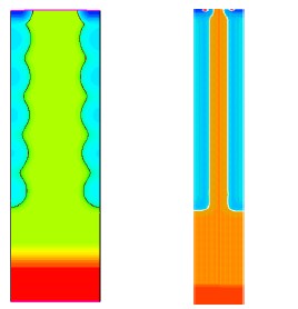
Fig. 3. Vertical structure of multiple epi superjunction technology (left) and deep trench epi-filled super-junction technology (right), not in same scale
As shown in figure 3, this new technology forms deep trench on N-type epi, and then fills it with Ptype epi. In this way, the new SupreMOSTM technology, has achieved much higher active cell density and simpler processes. The onresistance per specific area of new device is less than one fourth of standard power MOSFETs, and 40% smaller compared to previous generation SuperFETTM super-junction MOSFET. The reduced on-resistance of the new device is directly related to conduction losses in the interleaved LLC resonant converters.
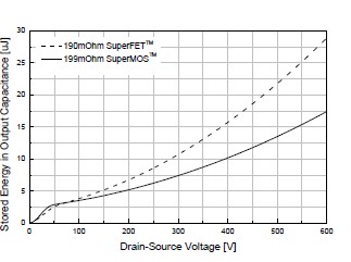
Fig. 4. Stored energy in output capacitance
In addition to lower on-resistance, another important parameter for a power switch that is going to be applied to resonant converter is less stored energy in the output capacitance. A device with less stored energy requires less resonant energy.This new technology achieved 35% less stored energy at for typical switching power supply bulkcapacitor voltage as shown in figure 4. Finally, life time control processes are added to this technology to form fast recovery body diode. Because this technology has higher cell density, there are more charges to be recovered at same area. Therefore, more precise control in process is required.
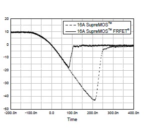
Fig. 5. Body diode reverse recovery characteristics
In figure 5, reduction of reverse recovery charge (Qrr) because of life time control is described at 200A/us of di/dt and 10A of forward current conditions. The smaller Qrr resulted in reduced peak reverse recovery current (Irm) that guarantees
rugged operation of LLC resonant converters. During start-up, over-load, or shorted output condition, operating point of LLC resonant converter could move into capacitive load region (zero current switching region) and high current spikes happen due to body diode reverse recovery. Because current peak is determined by Qrr and device failure depends on current level and junction temperature, reduced Qrr and Irm greatly improves system reliability. In addition, replacing existing power MOSFET with fast recovery type is very simple to implement and no additional circuitry is required.
4. Experimental Results
A 1kW rated interleaved LLC resonant converter has designed to verify benefits of the new SupreMOSTM FRFET MOSFET. Input voltage is set to typical PFC output voltage, 390VDC, and output voltage is set to 48VDC that is popular for telecom applications. An EER3543 core is used and transformer turn ratio has determined to 40:8. Resonant capacitance is set to 22nF. Design details of transformer and resonant tank parameters are shown in figure6.
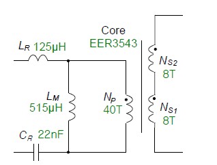
Fig. 6. Resonant tank of designed 1kW LLC converter
Figure 7 shows primary currents of two paralleled converters and output current. Primary currents are well kept with 90 degrees phase difference, and output current ripple is 13A peak-topeak at full load.
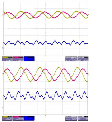
Fig. 7. Primary currents [CH1,CH2; 5A/div] and output current [CH3; 10A/div] at 500W (above) and 1kW (below)
Power conversion efficiencies are shown in figure 8. A 16A, 600V rated fast recovery type super- junction MOSFET is selected as primary switch from each technology. All measurements are done under natural convection cooling condition. The new device achieved 0.76% and 0.37% higher efficiency at 20% and 100% load respectively.
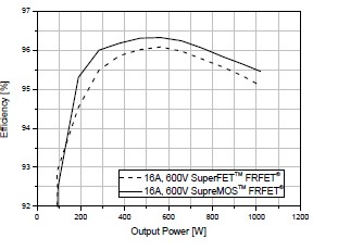
Fig. 8. Efficiency of the interleaved LLC converter
A new device utilizing deep trench epi filled super junction technology is discussed. It can improve system efficiency while providing rugged operation.
5. Literature
[1] Bo Yang, F. C. Lee, A. J. Zhang, and G. Huang: LLC Resonant Converter for Front End DC/DC Conversion, APEC 2002, pp.1108-1112 [2] K. Yi, G. Moon: A Novel Two Phase Interleaved LLC Series Resonant Converter using a Phase of the Resonant Capacitor, Journal of Power Electronics, Vol. 8, No. 3, July 2008 [3] J. Kim, S. Kang, B. Chung, E. Kim, D. Huh, Y. Jung: Two Phase Interleaved LLC Resonant Converter, KIPE Autumn Conference 2008, pp.115-117 [4] H. Figge, T. Grote, N. Froehleke, J. Boecker, P. Ide: Paralleling of LLC Resonant Converters using Frequency Controlled Current Balancing, PESC 2008, pp.1080- 1085 [5] M. Kim, W. Kang, M. Hallenberger: A New Way of Generating Gate Signals for Operating Two-Phase Interleaved Series Resonant Converters, PCIM Europe 2009 [6] W. Choi, S. Young: Improving system reliability using FRFET® in LLC resonant converters, PESC 2008, pp.2346-2351 [7] W. Choi, S. Young, D. Kim: Analysis of MOSFET failure modes in LLC resonant converter, INTELEC 2009