
Implementing Advanced Control Strategies for Phase Shifted Full-Bridge DC-DC Converters using Micro-Controllers
Hrishikesh Nene, Texas Instruments Inc., U.S.A., h-nene@ti.com
Abstract
This paper presents voltage mode control (VMC) and peak current mode control (PCMC) implementations for a phase shifted full-bridge (PSFB) converter in a highly integrated micro-controller based system. Adaptive zero voltage switching (ZVS) and various synchronous rectification schemes are discussed. Details for generating complex gate drive waveforms, required by such control schemes, and intelligent timing control, to optimize system performance under changing operating conditions, are also provided. Experimental results obtained using two PSFB systems (600W and 360W) are presented. A constant high system efficiency above 10% rated load, novel PCMC waveform generation,and simple system implementation are the highlights of this implementation.
1. Introduction
Phase shifted full bridge (PSFB) DC-DC converters are used frequently to step down high DC bus voltages and/or provide isolation in medium to high power applications like server power supplies,telecom rectifiers, battery charging systems, and renewable energy systems. Traditionally, microcontrollers have been restricted to only performing supervisory or communications tasks in these systems. With the availability of high performing micro-controller devices, it is now possible to use microcontrollers for closing control loops in these systems, in addition to handling the traditional microcontroller functions. These systems can implement advanced control strategies to optimally control the power stage under different conditions and also provide system level intelligence.
A PSFB converter consists of four power electronic switches (like MOSFETs or IGBTs) that form a full-bridge on the primary side of the isolation transformer and diode rectifiers or MOSFET switches for synchronous rectification (SR) on the secondary side. This topology allows all the switching devices to switch with zero voltage switching (ZVS) resulting in lower switching losses and an efficient converter. In [1-3], zero voltage switching operation of a PSFB stage is investigated. The main drawback here is that ZVS is sacrificed under low load operation. In [4-6], this limitation is overcome by adding additional components, which may not be always practical. In this work, ZVS for switches in the right leg of the full bridge and zero//low voltage or valley switching for switches in the left leg is achieved across the complete load range, by changing dead-times for primary side switches based on load conditions.For such an isolated topology, signal rectification is required on the secondary side. For systems with low output voltage and/or high output current ratings, implementing synchronous rectification instead of diode rectification achieves the best possible performance by avoiding diode rectification losses [7,8]. In this work, current doubler synchronous rectification is implemented on the secondary side with different switching schemes to achieve optimum performance under varying load conditions.
A DC-DC converter system can be controlled in various modes like voltage mode control (VMC), average current mode control (ACMC) or peak current mode control (PCMC). Implementing these different control modes for controlling the same power stage typically requires redesigning the control circuit along with some changes to the power stage sensing circuit. With a micro-controller based system, all these modes can be experimented with on the same design with minimal or no additional changes. Such a system (Fig. 1) is implemented here using VMC and PCMC control schemes.
PCMC is a highly desired control scheme for power converters because of its inherent voltage feed forward, automatic cycle by cycle current limiting, flux balancing and other advantages [9]. Implementing PCMC for a PSFB system requires complicated PWM waveform generation with precise timing control. A new approach to this waveform generation is presented using a micro-controller without requiring any additional support circuitry. Programmable on-chip slope compensation hardware is used to provide appropriate slope compensation that guarantees open loop stability and eliminates/limits sub-harmonic oscillations at the output. For PCMC implementation with a micro-controller, the regu lated output voltage is dependent on the amount of output voltage ripple, which in turn is dependent on the load. This relation is explained in detail and different solutions are suggested. Oversampling of the output voltage is recommended as the best option.
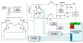 Fig. 1. PSFB System Block Diagram
Experimental results obtained using two PSFB systems (360W and 600W), developed as part of this effort, are presented. TMS320F28027 micro-controller is used in both cases. Peak efficiency greater than 95% and efficiency greater than 90% down to 10% load is achieved with the 600W PSFB system.
2. Operational Highlights
2.1. Voltage Mode Control (VMC)
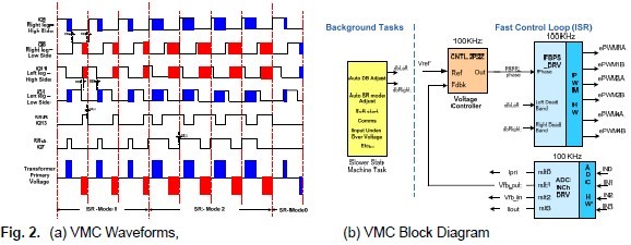
Fig. 1 shows the block diagram of a PSFB system, where MOSFETs Q11, Q1, Q2 and Q8 form a full bridge. Switches in each leg are driven with complementary pulse width modulated (PWM) signals of fixed (50%) duty cycle and frequency. Phase shift of the PWM signals driving switches in one leg of the bridge with respect to the ones driving switches in the other leg, dictates the amount of overlap between diagonally opposite switches. As seen in Fig. 2(a), longer the overlap between diagonal switches, longer the amount of time the input voltage is imposed across the transformer primary winding, and, thereby, larger the amount of energy transferred to the secondary. The controller regulates the output by controlling this energy transfer by way of directly controlling the phase shift between the PWM signals driving the two legs. Thus this phase shift is the controlled parameter. It should be noted that with VMC implementation there is a need to include a DC blocking capacitor in the transformer primary to avoid transformer saturation from flux imbalance over time.
Software is partitioned into a faster control loop ISR (Interrupt service routine) and slower background loop (Fig. 2(b)). In this case a 2-pole 2-zero compensator is used as the controller for the voltage loop.The phase command from the controller to the PWM decides the amount of energy transferred to the secondary. The background loop executes slower system level tasks like soft-start and shut-down routines, adjusting control loop parameters under different operating conditions, communications, deadband adjustment, synchronous rectifier switching scheme selection, among others.
2.2. Peak Current Mode Control (PCMC)
Implementing PCMC for a PSFB system requires complicated PWM waveform generation with precise timing control. A new approach to this waveform generation is presented here. As shown in Fig. 3(a),in every half switching cycle when the transformer primary current reaches the commanded peak reference value, one of the PWM waveforms driving the right leg switches (Q2/Q8) is ‘Reset’ immediately ending the power transfer phase. The PWM waveform driving the other switch in the same leg is ‘Set’after an appropriate dead-time (dead-band) window. Although not shown in Fig. 3(a) for simplicity, appropriate slope compensation is also provided that adds a ramp with a programmable negative slope to the peak reference current signal. This ‘Resetting’ and ‘Setting’ action of the PWMs in one leg results in a phase shift between PWM signals driving the two legs. The amount of this phase shift, and thereby the overlap between diagonal switches, is dependent on the amount of peak reference current. Higher the peak reference current, longer the overlap between diagonal switches, and thereby,more the energy transferred to the secondary. The controller regulates the output by controlling this energy transfer by way of controlling the peak reference current value. Thus this peak reference current is the controlled parameter. Unlike the VMC implementation, the DC blocking capacitor is not needed.
A 2-pole 2-zero controller is used as the controller for the voltage loop (Fig. 3(b)). The peak current reference command from the controller to the DAC dictates the amount of energy transferred to the secondary.
2.3. Zero Voltage Switching (ZVS) or Low Voltage Switching (LVS)
PSFB DC-DC converters make use of parasitic elements in the circuit to ensure zero voltage across the MOSFET switches before turning them ON. For the system discussed here, switching transitions on the right leg switches end the power transfer interval. When transitions on the right leg switches occur, current in the primary winding is close to its maximum magnitude for that half cycle. The reflected load current aids the circulating energy in the primary circuit during this time, which makes it possible for voltage across switches in the right leg to approach zero volts. It is possible to achieve ZVS for the right leg switches across the complete load range. It should be noted that as the load decreases the amount of dead-time for the right leg switches needs to be increased to achieve/approach ZVS. Switching transitions on the left leg switches start the power transfer interval. During the left leg switching transitions, primary current decreases. It crosses zero current value and changes direction.
This results in lower available energy for ZVS. In fact for switching transitions on the left switches under low load conditions, voltage across the switch may not go to zero before turning it on. Switching losses can be kept to a minimum by turning left leg switches ON at a time when the voltage across them is at a minimum. This is called valley switching or low voltage switching (LVS). As the load changes the time at which the left leg switch should be turned on to achieve LVS changes, requiring dead-time adjustment like the right leg switches.
2.4. Synchronous Rectification
The synchronous rectifiers can work in one of the following three modes at any given time:
I. Mode 0: This is the classical diode current doubler mode achieved by keeping synchronous rectifiers turned OFF. It is useful for very low load operations where synchronous rectifier switching losses are greater than the power savings obtained by synchronous rectification.
II. Mode 1: Useful when operating at very low to low loads. In this mode, synchronous rectifier MOSFETs are ON only when the corresponding diagonal bridge drive signals overlap.
III. Mode 2: Useful for all other load ranges. In this mode, synchronous rectifier MOSFETs are OFF only when the corresponding opposite diagonal bridge drive signals overlap.
Fig. 2 and Fig. 3 depict waveforms generated for driving the synchronous rectifier switches in these modes. It is important to implement mode transitions seamlessly without any glitches or anomalies on the PWM outputs even during large load transients to ensure safe operation of the system.
2.5. Output Voltage Regulation with Changing Load
The regulated output voltage is affected by changing load conditions. This problem exists because of ripple on the output voltage that appears at two times the switching frequency. At low loads, peak-to-peak voltage ripple is relatively small, while at higher loads it increases considerably. If the ADC conversions are triggered at a fixed point within a switching cycle, the sensed ADC voltage result is smaller at high loads (for the same average voltage). This is shown below:
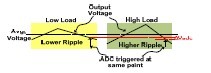
Fig. 4. Effect of fixed point ADC conversion triggering for output voltage sensing
Thus, for same average output voltage, a smaller output voltage is seen by the controller under high load operation. The controller compensates for this ΔVadc, which results in an increase in the actual output voltage value as the load increases. A few possible solutions are suggested here.
1. Start of ADC conversion can be triggered at an appropriate time in every half cycle so as to directly sense the average voltage. With PCMC duty cycle is not pre-determined and hence this trigger point is unknown. This method works very well with VMC and ACMC.
2. Average output voltage can be calculated at a slow rate and an outer slower loop can be used to adjust voltage reference or feedback. However, this may affect the dynamic performance.
3. The average output voltage can be calculated on a cycle-by-cycle basis by over-sampling it. There is minimal impact on the dynamic performance. This is the method recommended here.
4. Increased filtering at the ADC input can attenuate the ripple. However, this affects system dynamic performance, while the output voltage behavior still remains the same.
3. Results
Results are based on two 400V DC input to 12V DC output, PSFB systems. A PWM frequency of 150 KHz was used on the 360W board, while a PWM frequency of 100 KHz was used on the 600W board. The control algorithm was implemented on a Texas Instruments TMS320F28027 32-bit microcontroller, in both cases. Fig. 5 shows pictures of the two boards.
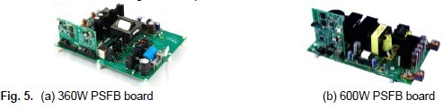
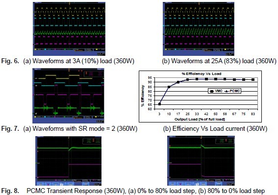
Fig. 6 shows transformer primary voltage, gate drives for diagonal switches and primary sensed current. Fig. 7(a) shows gate drives for Q11 and Q8, primary voltage and gate drive for SR switch Q7. As seen in Fig. 7(b), system efficiency remains almost constant at or above 93% for all loads greater than 20%, while the peak efficiency is around 94%. With both VMC and PCMC modes output peak deviations of less than 3% and settling times less than 180us are achieved for 0% to 80% (and vice-versa) step change in load (Fig. 8). PCMC step response looks like a damped first order system. Without synchronous rectification, the system efficiency drops by up to 5% under some load conditions. Adaptive ZVS switching significantly improves efficiency of the system across the complete load range.
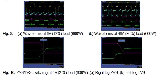
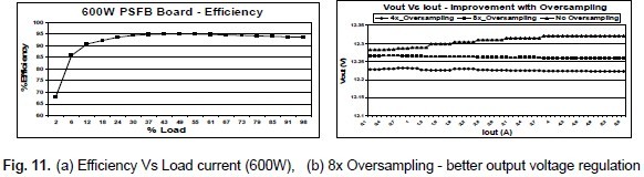
Transformer primary voltage, gate drives for diagonal switches and primary sensed current for the 600W board are shown in Fig. 9. Fig. 10 shows ZVS and LVS switching for the right and left leg switches under 1% load. This helps achieve high efficiency numbers shown in Fig. 11 (a). System efficiency of more than 90% is obtained for all loads greater than 10% rated load, while the peak efficiency is around 95%. Fig. 11(b) shows improvement in output voltage regulation with changing load by using 4x and 8x oversampling method. Without using the oversampling method, the 12V output voltage changes by about 40mV from 0A load to around 4A load. Changes beyond 4A load are not significant. With 8x oversampling, the 12V output voltage change is less than 7mV.
4. Summary
A digitally controlled PSFB DC-DC converter system was presented. VMC and PCMC control scheme implementations were presented along with ZVS, and different synchronous rectification modes for optimum system performance. A new method to generate PCMC PWM waveforms using a microcontroller was presented. This method uses on-chip PWM, comparator, DAC and slope compensation resources to implement PCMC without needing any external support circuitry. Experimental results obtained using both VMC and PCMC schemes suggest that system efficiencies obtained with these modes are almost identical to each other across the load range. ZVS and/or LVS switching is obtained across the complete operating range. This combined with implementation of different synchronous rectification schemes makes it possible to achieve high system efficiency across a wide load range.
Output voltage regulation issue with changing load was discussed and several solutions were suggested. The oversampling method provides a good solution to this problem as shown by experimental results. This micro-controller based implementation provides an ability to generate, and control, complex gate drive waveforms required for these control schemes while still providing a level of intelligence unique to digitally controlled solutions. It can be concluded that this work provides simple system level implementation by using a micro controller to handle the most complicated parts of PCMC and VMC schemes for PSFB converters.
5. Literature
[1] R. A. Fisher, K. D. T. Ngo, and M. H. Kuo, “A 500 kHz, 250 W Dc-to-DC converter with multiple outputs controlled by phase-shift PWM and magnetic amplifiers,” in Proc. High Frequency Power Conversion Conf., 1998, pp. 100–110.
[2] J. A. Sabaté, V. Vlatkovic, R. B. Ridley, F. C. Lee, and B. H. Cho, “Design considerations for highpower full-bridge ZVS-PWM converter,” in Proc. IEEE APEC’90, 1990, pp. 275–284.
[3] L. Mweene, C. Wright, and M. F. Schlecht, “A 1 kW, 500 kHz front-end converter for a distributed power supply system,” in Proc. IEEE APEC’89, 1989, pp. 423–432
[4] R. Ayyanar and N. Mohan, “A novel soft-switching dc–dc converter with wide ZVS-range and reduced filter requirement,” in Proc. IEEE PESC’99, 1999, pp. 433–438.
[5] “Full-load-range-ZVS hybrid dc–dc converter with two full-bridges for high-power battery charging,” in Proc. INTELEC’99, 1999.
[6] Baggio, J.E.; Hey, H.L.; Grundling, H.A.; Pinheiro, H.; Pinheiro, J.R.;” Isolated Interleaved-PhaseShift-PWM DC–DC ZVS Converter” Industry Applications, IEEE Transactions on Volume: 39 ,Issue: 6 2003 , Page(s): 1795 – 1802
[7] Balogh, L. “Design Review: 100-W, 400-kHz, DC/DC Converter With Current Doubler Synchronous Rectification Achieves 92% Efficiency”, Topic 2, SEM–1100 Power Supply Design Seminar Manual, Unitrode Corporation
[8] Steve Mappus, Texas Instruments, Application note SLUA287 – March 2003 “Control Driven Synchronous Rectifiers In Phase Shifted Full Bridge Converters”
[9] N.H. Kutkut, G. Luckjiff, “Current mode control of a full bridge DC-to-DC converter with a two inductor rectifier”, Power Electronics Specialists Conference, 1997. PESC '97, pp. 203 - 209 vol.1