
Optimized Design against Cosmic Ray Failure for HVIGBT Modules
Hitoshi Uemura*, Shinichi Iura*, Katsumi Nakamura*, Minho Kim**, Eugen Stumpf ***
* Power Device Works, Mitsubishi Electric Corporation, Fukuoka, Japan
Tel. +81 92 805 3395 Email: Hitoshi.Uemura@db.MitsubishiElectric.co.jp
** Fukuryo Semicon Engineering Corporation, Fukuoka, Japan
*** Mitsubishi Electric Europe B.V., Germany
Abstract
A phenomenon of failure for high voltage power semiconductors due to cosmic rays during high voltage applied operation was first described in 1994 [1-3] and has been examined. The phenomenon is a hard error called a Single Event Burnout (SEB), i.e. a permanent failure. The IGBT has become an in- creased voltage class up to 6.5kV and is not able to avoid the cosmic rayinduced failure issue. A High Voltage IGBT (HVIGBT) design has been focused on for taking into account Long-Term DC volt-age Stability (LTDS) against cosmic rays. This paper describes an improved design for LTDS of 6.5kV HVIGBT modules without sacrificing electrical performance and reports verification and analysis results for an accelerated neutron irradiation experiment.
1. Introduction
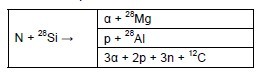
It is generally held that neutrons have the most impact on the cosmic failure rate for high voltage power devices. Neutrons with high energy (≥10MeV) are generated when cosmic rays collide with the atmosphere and the energetic neutrons are propelled to the ground. Furthermore, when highly energetic neutrons collide with nucleus of the silicon of a semiconductor substrate, certain kinds of ions are generated due to nuclear reaction as shown in Table 1. [4-5]
Table 1: Example of nuclear reactions with neutrons and silicon
Consequently, the generated ion behaves as a “carrier generator” in silicon, giving a lot of electrons and holes to the local region in silicon. This phenomenon leads to failure of high voltage power devices under high DC voltages. [5]
This report provides an optimized design and analyzes the result of the accelerated neutron irradiation experiment to improve the LTDS against cosmic ray-induced failure in high voltage power devices focusing on 6.5kV HVIGBT modules.
2. Chip design concepts for HVIGBT modules
The key robust design approach against cosmic ray induced failures in high voltage power devices is to reduce the maximum electric field strength during blocking voltage states. [3] Today’s major design rules as an effective countermeasure are:
(A) higher resistivity of N-based silicon
(B) thicker N- drift region
The above design method, however, has difficulties in improving electrical performance, especially power losses. The aim of designing newly developed high voltage power semiconductor chips for the latest HVIGBT modules is robustness against cosmic ray-induced failure without sacrifice of the electrical performances.
The newly developed IGBT, called Enhanced Light Punch Through IGBT: E-LPT, was designed with:
(A) a lightly doped thick N buffer combined with a shallow P collector
(B) a thin N- drift layer with a longer carrier lifetime
(C) a MOS gate cell with an additional N layer
A comparison of the IGBT cross-sectional view between E-LPT and a conventional Punch Through (PT) IGBT and the doping concentration at the collector side is shown in Fig. 1(a). [6]
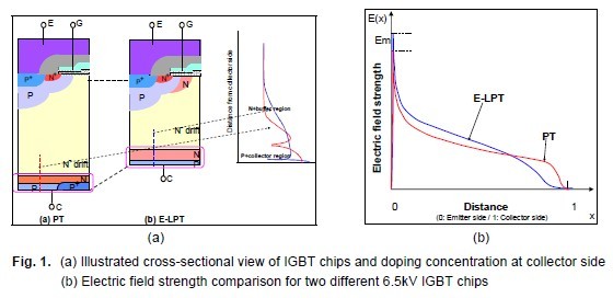
Fig. 1(b) illustrates comparison of simplified electric field strength for both IGBTs under the blocking DC voltage 6.5kV. The E-LPT has been designed optimizing the slope of the electric field strength, especially reduced around the collector side.
Moreover, the optimized wafer process, strengthened gettering, was adopted to minimize an impurity induced crystal defect in silicon.
A newly developed diode chip that is used as a free-wheeling diode has also been included in the LPT structure with optimized carrier lifetime control similar to E-LPT.
3. Verification of cosmic ray robustness by experiments
3.1. Experiment conditions
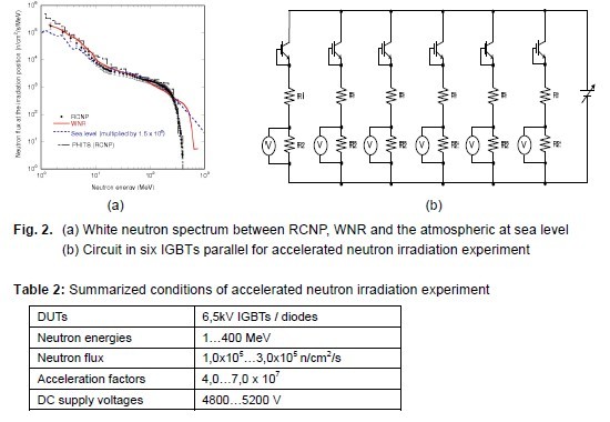
The neutron irradiation experiment was conducted at the Research Centre for Nuclear Physics (RCNP), at Osaka University in Japan, where the neutron beam spectrum closely matches the real atmospheric spectrum and that of a credible neutron facility, the Weapons Neutron Research Facility (WNR), Los Alamos National Laboratory, New Mexico, USA as shown in Fig. 2(a) [5].
CNP provides a well-defined white neutron beam with energies up to 400 MeV by using a ring cyclotron. The neutron beam flux was measured with a special recoil proton detector. The measured coefficient of accelerated neutron beam flux was 4,0…7,0x10⁷ times that at sea level in Tokyo, Japan.The experiment was carried out using both 6.5kV IGBT chips and diode chips, respectively, as Device Under Test (DUT). The supplied DC voltage for E-LPT was applied to several different voltage levels from 4800 V to 5200 V. Table 2 summarizes the experiment conditions and Fig. 2(b) shows the experiment circuit for IGBT chips
The DUT was connected to a maximum of six chips in parallel with a short between the gate and emitter. Two resistors (R1 and R2) were also connected to DUTs in series for circuit protection and leakage current (IR2) measurement during the experiment. The failure criterion used was IR2, which measured the voltage of R2 during applied DC voltage.
3.2. Experiment results
SEB time, the time until reaching the failure criterion, was recorded until all DUTs failed. A typical IR2monitoring result of 6.5kV E-LPT at DC supply of 5000 V is shown in Fig. 3(a).
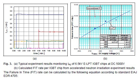

The calculated FIT rate per IGBT chip as a function of DC supply voltage is shown in Fig. 3(b). The FIT rate of E-LPT gives a drastically improved result approximately 1/10 lower at DC of 4800 V compared to conventional PT IGBTs.
4. Analysis of failed DUTs by neutron irradiation experiment
4.1. Observation of SEB failure spots
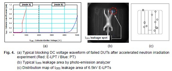
Fig. 4(a) displays typical blocking DC voltage waveforms between Collector to Emitter (VCES) of failed 6.5kV DUTs by the neutron irradiation experiment. All of the DUTs still have withstanding VCES voltages of around several hundred to a thousand, not shorted between Collector and Emitter. The withstanding VCES level can be classified into two failure modes as follows:
SEB with [mode A] : VCES < 2000V SEB with [mode B] : VCES≥ 2000V
E-LPT and conventional PT IGBT were clearly different failure modes shown in Table 3.
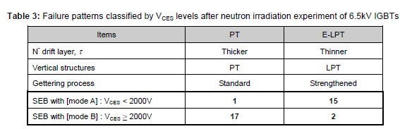
SEB failure spot was investigated from the top view (emitter side) by using a photo-emission analyzer to observe Collector-Emitter cut-off current (ICES) leakage area. The photo-emission analyzer can be detected visibly even if there is too small ICES such as nano-amperes. The failed 6.5kV E-LPT with [mode A] was investigated and the ICES leakage area was able to be observed in a very narrow area in the colored portion (in red circle) indicated in Fig. 4(b). The investigated distribution of ICES leakage area for the other failed 6.5kV E-LPT with [mode A] was random as shown in Fig. 4(c).
Consequently the SEB failure spot gives no correlation of failure root cause to the chip structure such as MOS gate and field limiting ring design due to random failures. [7]
On the other hand, the failed DUTs with [mode B] were not able to be observed in an ICES leakage area at the SEB failure spot with the photo-emission analyzer. The factors affecting it could be a dif ferent SEB failure spot between [mode A] and [mode B], i.e. SEB failure spots are on the top side (emitter side) for [mode A] and on the back side (collector side) for [mode B].
The depletion layer during the blocking voltage state expands from the emitter side toward the collector side. Due to the defective spot located on the emitter side for [mode A], the failure pattern of [mode A] indicates the possibility of faster reaching of the depletion layer to the defective spot under 2000 V than [mode B].
To determine the realized location of depth direction of the defective spot, the cross-section of failed 6.5kV E-LPT with [mode A] was investigated by using a Scanning Electron Microscope (SEM).
Fig. 5(a) shows obtained pictures from the analysis result, which indicated the red circle in Fig. 4(b).The defective point was found to be located approximately 40 µm in depth from the emitter side in the N- drift region and was 2 µm x 2 µm in size. In addition, a crack was barely visible with the picture on the periphery of the defective spot, and melted silicon also was confirmed. It is assumed that melted silicon was derived from local heating caused by concentrated leakage current.
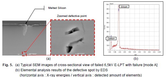
For further investigation, elemental analysis of the defective spot was performed with EDS (Energy Dispersive X-ray Spectroscopy) and the analysis result of detected element amount is shown in Fig. 5(b). There were two kinds of detected elements: one was of course silicon and the other was carbon.The other peculiar element was not able to detect by the EDS analysis. The detection of the carbon might be indicated due to the grinding sludge during the analysis.
4.2. Analysis by device simulations
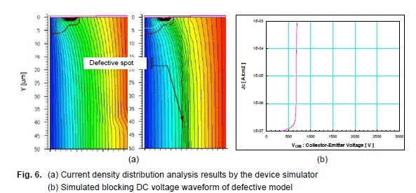
The current-density distribution of 6.5kV E-LPT IGBT was simulated to ascertain influence of the defective spot upon the blocking voltage characteristic by using the semiconductor device simulator. The defective spot, modeling by adjusted lifetime, was arranged at 40µm in depth from the emitter side similar to the analysis result in Fig. 5(a).
The un-uniform current-density distribution can be seen from the model with the defective spot in Fig.6(a) and Fig. 6(b), which display the simulated blocking DC voltage waveform.
A result was obtained similar to the blocking DC voltage waveform [mode A] in Fig. 4(a) increasing ICES suddenly at around 700 V.
5. Conclusion
New findings were obtained from analysis of the neutron irradiation experiment and the simulation result for 6.5kV IGBTs as follows:
a) VCES level of failed DUTs can be classified: [mode A] VCES < 2000V and [mode B] VCES≥ 2000V
b) Most of the failure pattern is different mode: [mode A] for E-LPT and [mode B] for conventional
c) The defective spot of [mode A]: 40µm in depth from the emitter side and 2µm x 2µm in size
d) No peculiar elements from the defective spot, only detected most of silicon and slight carbon
e) E-LPT has improved robustness factor of 1/10 against cosmic ray compared to conventional
The newly developed E-LPT IGBT has been improved the robustness against cosmic ray-induced failure in comparison with conventional IGBT by LPT structure with optimized carrier lifetime control. The key factors are the distribution of electric field strength, especially its slopes on the collector side, and minimized the crystal defect in silicon by the strengthened gettering during the wafer process. Conse quently the SEB failure spot moved from the collector side to the emitter side proved by the analysis of the neutron irradiation experiment and the simulation results.
To summarize converting FIT rates for modules, the latest 6,5kV HVIGBT module (rated 750A) with newly developed E-LPT IGBTs and diodes with 18 chips each has improved DC supply voltage ap proximately 200V at 100FIT (Failure In Time) compared to conventional HVIGBT modules.
6. Literature
[1] H.Kabza, et al: Cosmic Radiation as a Cause for Power Device Failure and Possible Counter-measures: ISPSD, 1994
[2] H.Matsuda, et al: Analysis of GTO Failure Mode during DC voltage blocking: ISPSD, 1994
[3] H.R.Zeller: Cosmic Ray Induced Breakdown in High Voltage Semiconductor Devices, Microscopic Model and Phenomenological Lifetime Prediction: ISPSD, 1994
[4] C.Findeisen, et al: Extrapolation of cosmic ray induced failures from test to field conditions for IGBT modules: Microelectronics Reliability, 1998
[5] K.Sugimoto, et al: Errors and Failures Caused by Terrestrial Neutron Induced by Cosmic Rays:Semiconductor devices and materials forum in Kumamoto, 2010
[6] K.Nakamura, et al: Impact of an LPT(II) Concept with Thin Wafer Process Technology for IGBT’s Vertical Structure: ISPSD, 2009
[7] S.Nishida, et al: Cosmic Ray Ruggedness of IGBTs for Hybrid Vehicles: ISPSD, 2010