
Davide Chiola, Infineon Technologies Austria, Siemensstr. 2, 9500 Villach, Austria
Holger Hüsken, Infineon Technologies, Am Campeon 1-12, 85579 Neubiberg, Germany
Thomas Kimmer, Infineon Technologies Austria, Siemensstr. 2, 9500 Villach, Austria
Abstract
The IGBT is traditionally the device of choice in low switching frequency applications like Inverter-driven Motor Drives thanks to its low conduction losses. At the same time the IGBT can be operated at high current density, hence it provides a cost effective-solution were higher power density and lower cost are required. For this reason its utilization also in higher switching frequency applications like SMPS, UPS, Welding, Induction Heating and more recently Solar Inverters has been considered. We present in this paper the 3d generation of 600V High speed IGBT (“H3” Product family) from Infineon Technologies optimized for high frequency hard-switching applications. The main device features are reviewed, and the benefit for the target applications are highlighted.
1. Introduction
High Energy efficiency standards set by Governmental Agencies and lower system costs are the main driving forces toward development of more efficient power switches [1]. System designers have to carefully select the right switch in order to meet both requirements: in high power (> 5kW) systems, IGBT or Bipolar Transistors are typically adopted. In “low power” (< 2 kW) systems at Voltage below 1000V, MOSFETs are typically preferred were wide line or load variations and high switching frequency (> 150 kHz) are required: typical application are hard switched or ZVS SMPS, for example. In the same power class IGBTs are typically adopted at lower switching frequencies (< 40kHz) and where narrow line or load variation have to be covered: typical applications requiring “hard” switching are Motor Drive, Uninterruptable Power Supply and Welding. Although several manufacturers are offering IGBTs designed for switching frequency even above 100 kHz, their wide adoption has been somehow limited by the difficulty to provide wide-load efficiency as required by recent energy efficiency regulations. Utilization above 40 kHz is observed however in resonant topologies like Induction Heating and microwave oven thanks to the adoption of “soft” switching, with ZVS or ZCS schemes [3].
Recent generations of IGBTs have two distinctive features that are pushing system designer to extend the range of utilization to higher switching frequency also in hard switching topologies: typically the IGBT die size is approx 1/3 of a MOSFET with equivalent current rating, reducing capacitance and gate charges for equivalent cell design, and the Vcesat - Eoff trade-off can be tailored to the required switching frequency by tuning a relatively small set of process anddesign parameters. New families of high speed IGBTs allow system designers to increase the switching frequency of the power transistors without changing the cooling requirements: an overall system cost reduction is therefore achievable, by reducing the cost of power switches and the size and cost of passive components.
On these motivations Infineon technologies have developed the third generation of High Speed IGBT, optimized for high switching frequencies, hard switching applications like Welding, Solar and UPS.
Above 20 kHz, the switching losses are typically dominating the overall losses, therefore reduction of Eon and Eoff without penalizing significantly Vcesat has been one target of the development. Second objective has been to avoid ringing and maintain smooth switching waveform with low dV/dt and dI/dt typical of Infineon IGBTs, to allow reduced EMI and less filtering.
In order to reduce Eoff losses in hard switching conditions, tail current at high temperature has to be eliminated, since these small losses are adding-up at high switching frequency. To reduce Eon losses, the IGBT design and the freewheeling diode have to be optimized.
2. TrenchStopTM
Technology In order to achieve these technical goals, the Trench Field Stop (TrenchStopTM) is the selected technology, like most of the recently released IGBT families from Infineon Technologies [4, 5]. Unlike other direct competitors, realizing fast IGBTs with planar cell, we demostrated that an optimized TrenchStopTM structure (Figure1) can still provide superior cost / performance trade-off also in high switching frequency applications.
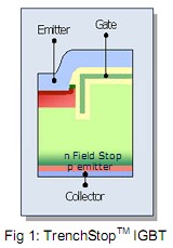
The combination of trench cell and field stop structure allows to tailor the plasma concentration inside the chip: a relatively higher plasma density in proximity of the trench gate allows reduced Vcesat, that means higher current density, therefore smaller chip area and lower cost. Modern implantation and annealing techniques allow the realization of regions of low carrier lifetime in proximity of the backside p-emitter: in combination with a reduced backside p-emitter doping and optimized field stop, this allows fast plasma extraction during turn-off and reduced current tail, still maintaining soft switching behavior. Special care was taken from the process point of view to make sure that such a weak emitter is still stable against process variations and a tight parameter distribution is achieved.
3. Dynamic characterization
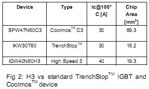
The switching behavior of the resulting device was compared against the standard TrenchStopTM IGBT3 technology and a CoolmosTM C3 with similar current rating (Figure 2) in a half-bridge hard switching test circuit with inductive load. The freeweehling diode is an 8A rated SiC Schottky diode from Infineon for all devices.
The CoolmosTM C3 was selected as a benchmark for fast switching performance. The resulting turn-off switching waveforms are shown in Figure 3 and 4. The typical half-bridge IGBT switching circuit is not designed for testing the CoolmosTM (Source pin as well as other parasitic inductances has to be reduced by special sockets and optimized board layout for Coolmos testing), hence for the comparison with CoolmosTM C3 the Gate Resistance Rg had to be increased (42 Ohm vs 11 Ohm) to avoid current and voltage oscillations:
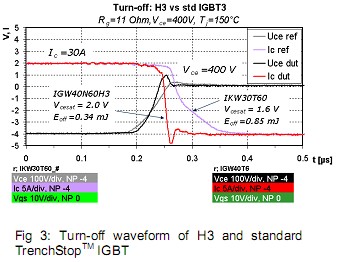
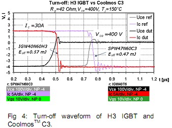
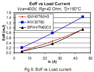
The current waveforms of the H3 IGBT are clearly showing the total absence of current tail at high temperature (Fig 3), and turn-off switching behavior that resembles the one of a unipolar fast switching device like the CoolmosTM C3 (Fig 4). The turn-off Energy is reduced by 60% compared to the std TrenchStopTM IGBT3 for a corresponding increase in Vcesat of 25%. In these test conditions, the 40A rated H3 IGBT is actually showing faster dI/dt at turn-off than the 30A CoolmosTM C3 (2080 vs 1000 A/us in the above graph), still showing smooth switching behavior and a moderate voltage overshoot of 100V. The CoolmosTM C3 still results in 17% lower Eoff due to the steeper voltage raise. A complete comparison at different load currents in shown in Figure 5:
A complete competitor evaluation is performed with the same test circuit and the resulting Vcesat/Eoff trade-off diagram is illustrated in Figure 6.
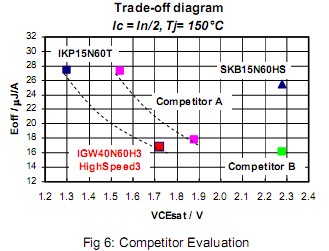
In order to represent a realistic application condition, the load current is half of the nominal current, since especially at high switching frequency some current de-rating may be required. Due to the different die size of the device under test, the Eoff losses are scaled by current rating.
The H3 IGBT shows the best trade-off point, with 170 mV lower Vcesat and 6% lower Eoff than the best competitor. The trade-off diagram clearly indicates the supremacy of selected design combination trench gate + field stop: the IKP15N60T and IGW40N60H3 are realized on the same TrenchStopTM technology base and offer the best trade-off curve, drastically reducing Vcesat and slightly Eoff compared to Competitor A, realized with planar gate + Field Stop. The Infineon SKB15N60HS and Competitor B are also high speed devices, realized however in NPT (Non Punch Through) technology, suffering from significantly higher Vcesat.
4. Diode selection
For application were a freewheeling diode is required, the High Speed 3 IGBT is paired with the 600V Emitter Controlled Diode of 3dgeneration. For the die size selection, we considered that in most of the target applications, like solar and UPS inverter, the energy flow is unidirectional, (from the load to the grid for solar inverters, for example). This result in a reduced stress on the diode compared to motor drive inverters with half-bridge configuration, were in “braking” mode (cosφ < 0) a high thermal stress is induced in the diode by the power dissipationin forward conduction. Another important difference to motor drive application is the current waveform through the IGBT: in typical single and dual transistor topologies in SMPS, PFC and welding, for example, there is usually a triangular or trapezoidal current waveform. The IGBT is hard commutated with turn-on currents lower than turn-off, therefore the current rating of the diode can be reduced, contributing to a reduction of the overall switching losses.
The effect of different diodes on the turn-on behavior of the 30A H3 IGBT is investigated in Figure 7
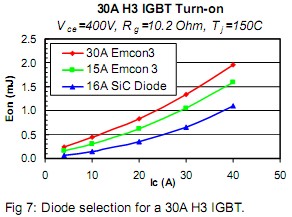
Although the SiC Diode provides 50% reduction of IGBT turn-on losses, the “15A” Emcon3 was selected to allow faster turn-on and keep a lower product cost. The high ruggedness and power handling capability of the Emitter Controlled 3rd generation series allows an increase of the switching current density. The inherent diode softness allows to reduce Rg,on and therefore the IGBT turn-on losses still maintaining good EMI behavior.
5. Loss breakdown
The breakdown of power losses for a single device in a real application is simulated for a 40A rated device in the following conditions (Figure 8): Ic=40A, Vdc = 400V, Rg,on=6.9 Ω, Rg,off=3.2 Ω, Duty Cycle=0.5, Tj=150C, fsw=20 kHz and 40 kHz, square pulse hard switching (full load current turn-on and turn-off):
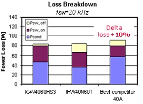
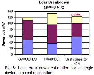
The H3 IGBT provides 10% and 4% lower losses at respectively 20 and 40 kHz compared to the best competitor, thanks to the reduced Eoff losses. At 20 kHz the conduction losses are still contributing to ~50% of the overall losses,therefore also the standard TrenchStopTM IKW40N60T shows similar losses thanks to the lower Vcesat. The analysis clearly shows how for these fast switching IGBTs the switching losses are dominated by Eon losses, indicating a direction of further improvement for the future.
6. In-circuit test
In order to assess the performance of the High Speed3 IGBT in a fast switching application, 20 and 30A devices were tested in a PFC test board, normally used for efficiency measurements of CoolmosTM at Infineon Technologies (Figure 9).
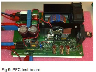
The board is designed for 1 kW, 400 V output, 110 to 230 V input voltage in CCM mode (Continuous Current Mode). The controller allows to change the switching frequency from 60 to 300 kHz. The DUT case temperature is maintained at 40°C by combined heater + fan control. The PFC choke is 1 uF and the boost diode is a 6A SiC Schottky IDT06S60C for all groups. The AC source is a Chroma 6530 and the DC load a Chroma 63202. The efficiency is measured with a Siemens Power Analyzer B6040.
The H3 IGBT is compared to a CoolmosTM C3 and other conventional (non Super Junction) MOSFET from competition (figure 10)
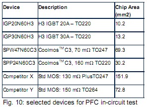
Due to the relatively big chip size of the devices under test, only measurements a low line (115V input) are performed; even in this case at max output power of 1 kW the load current is approx 10A, corresponding to 1/2 to 1/3 of the rated current of the selected devices. Results are summarized in figure 11 and 12:
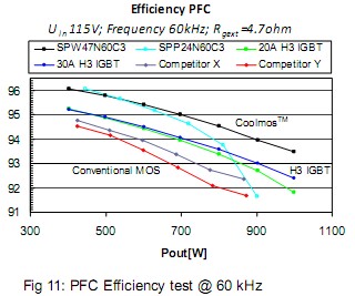

At 100 kHz the output power was limited at 600W in order to avoid thermal runaway.
The 70 mΩ CoolmosTM C3, best in class in TO247 package, shows the best efficiency at high load current above 600W. The H3 IGBT in TO220 clearly outperforms conventional MOSFETs in much bigger packages at both 60 and 100 kHz, utilizing 1/7 to 1/10 of the chip area. Despite having less than half of the chip area, the H3 IGBT outperformes also the 160 mΩ CoolmosTM C3 above 850W, clearly showing the power density advantage of this high speed IGBT
technology, and indicating a cost effective solution for high power PFC application above 1kW (telecom SMPS, for example).
At 60 kHz the 30A H3 IGBT provides some advantage over the 20A at high load, due to the lower Vcesat and Rthjc. The turn-off switching waveforms captured during the test at 60 kHz are shown in figure 13:

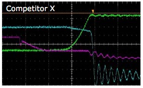
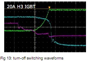
With an external gate resistance of 4.7 Ω the H3 IGBT shows smooth current waveforms with absence of ringing or oscillations, and no voltage overshoot, that would result in reduced EMI. Despite the bigger chip size that would require a small Rg to minimize the gate drive current, both the Coolmos and the conventional MOS instead show a snappy turn-off, that can be improved by increasing the turn-off gate resistance at the expense of increased losses. The possible reduction of the gate resistor thanks to the smooth switching behavior or the High Speed 3 IGTB translates in lower losses, resulting in lower system cost by reduction of cooling and filtering efforts.
7. Conclusion
In summary, we have presented the new 600V High Speed 3 IGBT from Infineon Technologies in the voltage class 600V, called “H3”. The new device provides benchmark performance and constitutes a cost effective solution in Solar, UPS,Welding and SMPS applications.
The dynamic characterization shows a total absence of current tail even at elevated temperatures, resulting in turn-off behavior very similar to a CoolmosTM device. The type and rating of the freewheeling diode was selected based on the requirements of the target applications. Finally, an in-circuit evaluation was performed in a PFC test board, showing superior efficiency compared to conventional MOSFETs of much bigger die size over a wide load range, and smooth switching behavior with absence of current oscillation and voltage overshoot even at low gate resistance, making the H3 IGBT an ideal solution to improve system efficiency and reduce system cost.
8. Literature
[1] Examples of Energy saving regulations by Agency are (visited March8th, 2010):
• Energy Star (http://www.energystar.gov)
• 80plus (http://www.80plus.org)
• CECP (China Energy Conservation Project http://www.cecp.org.cn)
[2] T. Kimmer, J. Oehmen; P. Tuerkes, S. Voss: " Reverse Conducting IGBT - A new Technology to Increase the Energy Efficiency of Induction Cookers "; Power Electronics Specialists Conference, 2008. PESC 2008. IEEE
[3] T. Laska, M. Münzer, F. Pfirsch, C. Schaeffer, T. Schmidt: " The Field Stop IGBT: a new Power Device Concept with a Great ImprovementPotential "; Proceedings ISPSD 2000
[4] H. Rüthing, F. Umbach, O. Hellmund, P. Kanschat, G. Schmidt: " 600V-IGBT3: Trench Field Stop Technology in 70 μm Ultra Thin Wafer Technology " Proceedings ISPSD 2003