
Comparison of the Output Power of RC-IGBT and IGBT / Diode Inverters
Hans-Günter Eckel, Daniel Wigger
University of Rostock, Germany
Tel. +49 381 498 7101
Fax +49 381 498 7102
hans-guenter.eckel@uni-rostock.de
Abstract
Reverse conducting IGBT (RC-IGBT, also called BIGT) combine the functionality of an IGBT and a diode in a single chip. For a better understanding of the advantages of RC-IGBT in comparison to conventional IGBT / diode modules, this paper separates between the electrical and the thermal effect of the RC-IGBT. The electrical effect addresses the differences of the on-state voltage and the switching losses, it is device specific. The thermal effect addresses the advantage due to the integration of the IGBT and diode functionality in one chip, it is application specific.
1. Introduction
Reverse Conducting IGBTs (RC-IGBT), also called Bi-Mode Insulated Gate Transistors (BIGT) with blocking voltages in the kV-range are relatively new devices [1], [3], [5]. They combine the functionality of an IGBT and its antiparallel free-wheeling diode in a single chip. This is realized by anode shorts in the backside emitter of the IGBT-chip. A 190 mm x 140 mm RC-IGBT module contains e.g. 36 RC-IGBT chips instead of the 24 IGBT-chips and 12 diode-chips of a conventional module. This may lead to different advantages of a RC-IGBT module compared to a conventional IGBT / diode module [2]:
- The current density in the IGBT-mode as well as in the diode-mode is considerably reduced. This reduces the on-state voltage of the device. As the active chip area is increased, the turn-on losses and reverse recovery losses are increased, if the emitter efficiency of the chips is the same. By an appropriate mixture of a chip area with and without anode shorts and by lifetime killing in the p-well, the relation between on-state and switching losses can be controlled. These advantages in the electric data are called the “electrical effect” of the RC-IGBT in this paper.
- As the whole chip area is active in the IGBT mode and in the diode mode, the output power of the inverter is significantly increased in applications, where the losses in the IGBT and diode don’t fit to the 2:1 chip area ratio of a conventional module. An extreme example is an inverter with a dc-output current. This is called the “thermal effect” of the RC-IGBT in this paper.
All measurements were done with 3.3 kV IGBT and RC-IGBT and scaled to a module in the standard 190 mm x 140 mm housing.
2. Electrical effect
2.1. Thermal model for calculation of the electrical effect
The electrical effect can be separated from the thermal effect by using an artificial thermal model, which consists only of one common thermal resistance for the IGBT and diode power loss [Eq. 1]. The same model with the same values is used for the RC-IGBT, where it describes the real situation [Eq. 2].
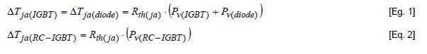
The larger the ratio between the thermal resistance between junction and case and the total thermal resistance between junction and ambient, the larger is the difference between the real thermal model and this artificial thermal model. So for very poor cooling conditions (e.g. natural cooling), this artificial model is not far away from reality.
2.2. Scaled RC-IGBT
To get a first impression of the potentials of RC-IGBT it is helpful to scale the electrical data from a state-of-the-art IGBT and diode, as it is done in Table 1. It is assumed, that this artificial RC-IGBT (called scaled RC-IGBT) has the same on-state voltage in the IGBT-mode as the conventional IGBT and in the diode mode as the conventional diode at the same current density in the chip. Furthermore,it is assumed that the scaled RC-IGBT has the same dependence of the turn-off losses on the chipcurrent as the conventional IGBT, the same dependence of the reverse-recovery losses on the chipcurrent as the conventional diode and that the turn-on losses are proportional to the reverse recovery losses.
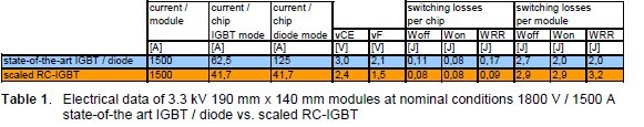
recovery charge are not proportional to the current. At lower current, the losses per current are higher than at higher current. The reverse recovery charge at 1/3 nominal current is more than 50% of the charge at nominal current. So three chips in parallel operating in the diode mode, will have more than 150% of the charge of one diode chip with the same current. The reverse recovery losses per chip are reduced to 50%, whereas the reverse recovery losses per module are increased to 150%. The turn-on losses are also increased by a factor of 1.5 (the proportionality between reverse-recovery and turn-on losses was an assumption). As the number of chips operating in the IGBT mode is also increased by a factor of 1.5, the turn-on losses per chip stay constant.
It must be remarked, that this scaled RC-IGBT is already a very ambitious device. The possibilities for separate optimization of the IGBT and the diode mode are restricted, as this is only one device. So the same thickness, the same doping of the base and the same charge carrier lifetime are mandatory.
2.3. Realistic RC-IGBT
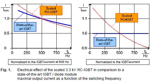
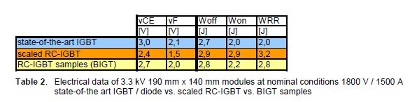
The results of Fig. 1 have already shown, that the RC-IGBT should have lower switching losses compared to the scaled approach. This was realized with the first high voltage RC-IGBT samples (3.3 kV BIGT devices, Table 2). The on-state voltage is only slightly lower than with the conventional IGBT, the turn-off losses are nearly the same, the turn-on losses are a little bit higher, the reverse-recovery losses are still significantly higher. Compared to the scaled RC-IGBT, the break even point in output current remains at 500 Hz. At higher switching frequencies, the disadvantage over the conventional IGBT is lower, at lower frequencies the advantage is lower.
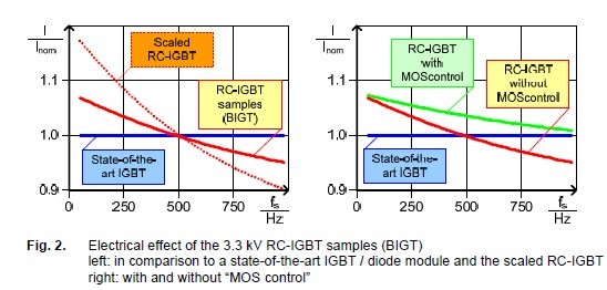
Using “MOS control”, the electrical effect gives an advantage of 2% to 7% in the relevant switching frequency range. An efficient MOS control is the key for good electrical data of an RC-IGBT.
3. Thermal effect
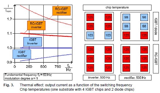
To separate the thermal from the electrical effect, an artificial RC-IGBT with the same electric values on module level in the IGBT mode as the conventional IGBT and in the diode mode as the conventional diode is introduced. Now, differences in the output current are a consequence of the better power loss distribution of the RC-IGBT. The advantage of the RC-IGBT due to the equal loss distribution over all chips depends of course on the inhomogeneity between IGBT and diode in the conventional module. The more the loss ratio differs from the 2:1 chip area ratio between IGBT and diode, the larger is the temperature inhomogeneity and the larger the advantage of the RC-IGBT. The loss ratio depends on the electrical data of the IGBT and the diode in the conventional module, on the inverter type, the operating point and the thermal behaviour of the inverter. The better the cooling, the higher is the temperature drop between junction and case and the higher is the advantage of RC-IGBT. For these investigations, a high performance water cooler was taken. With air cooling, the temperature drop between case and ambient is higher and the advantage of the RC-IGBT is lower.
The effect for inverter operation of a three phase VSI is shown in Fig. 3. The thermal effect is between 8% and 10%. The value is relatively low, because the conventional module fits quite well for this application and only one third of the chips are not fully utilized.
The situation is different in rectifier operation. Now, two third of the chips are not fully utilized. With the conventional module, the output power is 5 to 10% lower than at inverter operation. With the RC-IGBT, the output power in the rectifier operation is 10% to 20% higher than in inverter operation. So the RC-IGBT allows 20% to 40% more output current in comparison to the conventional IGBT / diode module in rectifier operation due to the thermal effect.
In Fig. 4 not only the fundamental frequency but also the modulation degree is low, which is typical for electrical drives at low speed. So both the IGBT and the diode have a turn-on time of about 50%. With the conventional module, this leads to a mean loss ratio of 2:1 between IGBT and diode, so the maximal IGBT and diode temperatures are nearly the same. The RC-IGBT has the same thermal resistance in the IGBT- and the diode-mode. So the lower losses in the diode-mode lead to a lower chip temperature when the device is operating in the diode-mode. This allows the modulation of a third harmonic on the output voltage, shifting the losses from the IGBT-mode into the diode mode and leading to 30% more output current than with the conventional IGBT / diode [2].
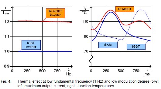
These examples show that the thermal effect is especially strong, if the diode is limiting the output current of the inverter.
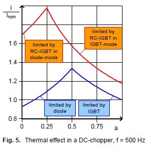
Another situation where the diode is limiting is the surge current stress. With the RC-IGBT, the chip area which can handle the surge current is increased by a factor of three. So if it is assumed, that the limiting temperature is the same for the conventional diode and the RC-IGBT in diode mode (which is a best case approximation), the surge current capability of the module would be increased by 80% only by the thermal effect (Fig. 6). This is an increase in i²t of more than factor 3. The electrical effect is still neglected, which is a worst case approximation.

4. Conclusion
The calculations with separated thermal and electrical effect show, that today’s RC-IGBT profit mainly from the thermal effect. The advantage depends strongly on the application. For the most important inverter application it is relatively small, because the conventional module is optimized for this application. For applications or operating points where the diode is limiting, the RC-IGBT shows a huge advantage.
5. References
[1] M. Rahimo, U. Schlapbach, A. Kopta, J. Vobecky, D. Schneider, A. Baschnagel “A High Current 3300V Module Employing Reverse Conducting IGBTs”, ISPSD 2008.
[2] H.-G. Eckel; “Potential of Reverse Conducting IGBTs in Voltage Source Inverters”, PCIM 2009.
[3] M. Rahimo, U. Schlapbach, R. Schnell, A. Kopta, J. Vobecky, A. Baschnagel; “Realization of Higher Output Power Capability with the Bi-Mode Insulated Gate Transistor (BIGT)“ EPE 2009.
[4] D. Wigger, H.-G. Eckel; “Comparison of the Power Cycling Stress between IGBT and BIGT Inverters”, PCIM 2010.
[5] A. Kopta, M. Rahimo, R. Schnell, M. Bayer, U. Schlapbach, J. Vobecky, D. Schneider; „The next generation 3300V BIGT HiPak modules with current ratings exceeding 2000A“ PCIM 2010.