
Digital power controller for improvement of converter efficiency
Bernhard Strzalkowski
Analog Devices
Wilhelm-Wagenfeld-Str.6
80807 Munich, Germany
Email: bernhard.strzalkowski@analog.com
Abstract
The benefits of digital power have been recognized for last years, the technology has been evolved into a state that allows its practical and efficient application. In the latest generation of digital power controllers, simple graphical user interfaces (GUI) has replaced in-depth software coding.
This article wil discuss the new possibilities for simply and comfortable design of high efficient power converter. It wil be presented, how to choose the optimal dead time of synchronous rectifiers (SR) without sensing drain source voltage. Output current sensing allows reduction power losses at light load and al ows introduction of adaptive dead time control.
Experimental results performed on digital y controlled full bridge forward converter Uin=48V,Uout=14V/25A demonstrate practical implementation of dead-time optimization algorithm.
1. Introduction
1.1. Synchronous rectification control methods overview
Because of significantly lower conduction losses, synchronous rectifiers are now used in low voltage DC power supplies including converters for telecommunication infrastructure, for battery operated electronics and for point-of-load circuits. Control of the synchronous rectifiers (SR) in forward converters has been accomplished in many different ways, from self-driven to complexly controlled techniques. Most existing control techniques allow the synchronous rectifier’s body diode to conduct for some small time interval, thus degrading efficiency. SR drive signal can be obtained through two ways: self-derived and external-controlled. Self-derived method develops SR gate drive signal by detecting either the current flowing through SR [1],[2] or the voltage drop across SR [3],[4]. Externalcontrolled method can also develop SR drive signal from the voltage signal that exists in the switching topology and adjusts to the desired drive timing. Many researchers exanimate voltage-driven synchronous rectification [5]–[7].Circuit implementation and operation are generally known. Recently, some new approaches to reduce the dead time have been introduced. The dead times are adjusted
adaptively to minimize the duty-cycle command, which results in maximization of the converter efficiency. Proposed schemes for improved synchronous rectifier commutation have been based on the idea that the synchronous rectifier should switch as an ideal rectifier: it should be turned on exactly at the time when the voltage across it drops to zero, and it should be turned-off exactly at the time when the current through it drops to zero [8]. Direct implementation of this idea requires fast sensing the zero-crossing of the voltage across the SR.
Some methods are particularly well suited for digital controller implementation by using predictive gate drive technique [9] or by using minimizing duty-cycling command [10].
The focus of this design review is a simple control algorithm and adjustment procedure, which elimi nates body diode conduction in synchronous rectifiers.
1.2. DPWM utilizing state machine for generating dead time
High efficient and high power densities converters utilize double-ended topologies, such as push-pul ,half-bridge and full-bridge. These topologies are increasingly popular in many applications such as telecom and computer [11]. The full-bridge converter with central taped synchronous rectifier has been chosen for examination the ability of digital power controller to minimize converter power losses. The Fig.1 shows the circuit diagram using a new digital power controller ADP1043, which utilize a state machine to generate control signals for full-bridge switches TA, TB, TC, TD and for synchronous rectifier SR1, SR2.
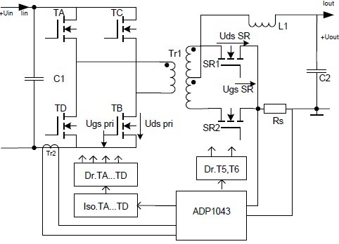
Fig. 1. Block diagram of high efficient full bridge digital power converter with centered tapped synchronous rectifier
The controller is able to perform predefined dead-time periods between any two edges of up to seven independent DPWM channels. The implemented DPWM’s provide very accurate adjusting of the SR control signal in respect to the signals generated for the full bridge MOSFET’s. The edge adjusting accuracy is 5ns for the whole frequency range 50 kHz to 625 kHz. The adjusting can be performed on the fly by means of the comfortable GUI, which executes the command to the digital control er by I2C bus [12]. The control er has two individual inputs for sense, protection and control of input and output current. The output current information can be use to introduce SR adaptive dead-time control.
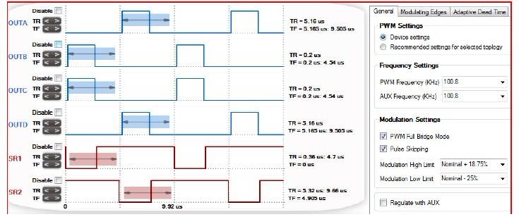
Fig. 2. The view of GUI details, showing set-up of DPWM’s and SR’s wave-forms
Simple graphical user interfaces (GUI) has been developed to program some registers of the state machine ADP1043A. Fig.2 shows the GUI screens shoot for programming desired fixed and variable periods of dead-times. Those variable periods are adapted to the fixed periods, when the predefined output current threshold is achieved. At light load condition, the losses caused by switching and driving of SR’s overweigh the switching and conducting losses when only the body diodes work as rectifier. The ADP1043A can disable SR as well as enable pulse skipping mode when output current undercross programmed threshold. In next chapter, the method of reducing power losses in synchronous rectifier is presented in user friendly balance between accuracy and practical simplicity.
2. Control method to reduce SR power losses
2.1. SR disabling at light load
The efficiency optimizing of full bridge power forward converter with synchronous rectification is not an easy task. The list of components dissipating power in DC/DC converters is long; not only component’s selection is critical, bud also optimizing control and modulation methods are time consuming process [13], [14]. At light load condition, the losses caused by switching and driving of MOSFETs overweigh the conduction losses when only the body diodes work as rectifier. As the power density and compactness of modern converters increases, so is being more difficult to measure waveforms for optimizing power efficiency. Introducing voltage- and current probes into the converter circuit cause additional inaccuracies of measured wave-forms and generate additional power losses.
A comfortable method to find out the break-even point for enabling/disabling of SR is using the GUI of ADP1043A. On measure the power dissipation for all load condition when the SR are enabled and then when SR are disabled. Only on mouse click is required to precede it. The plot of power efficiency versus output power shows the threshold value for enabling/disabling SR. The Fig.4 shows plot power losses versus output power for a quarter Brick full bridge 300W converter, performed by above described method.

It is visible that, for output power below 30W, the SR disabling reduces the power losses from 6 W down to 1W in Stand-by mode.
2.2. Determination optimum SR dead time
It is wel known that optimum switching of synchronous rectifier depends on the ability to adjust the dead-times during turn-off and turn-on. Too long dead times result in additional losses due to the body diode conduction and the body-diode reverse recovery. Too short dead-times may result in simultaneous conduction of the main switches and the synchronous rectifier, with even more power losses or result in converter destroying. In the presence of parameter tolerances, temperature variations and operating point changes, the simplest approach of fixed dead times often yields severely degraded efficiency, especial y in converters operating at relatively high switching frequencies. For the converter start-up procedure, it is highly recommended to choose relative long dead-times in order to measure and observe the SR wave-form without jeopardy of their destroying. Fig.3 shows the wave-forms of mains switch TB and SR1 (Fig.1) during start-up phase.

Fig. 4. The wave-form of main switch and SR during start-up phase, when dead-time between UgsSR and Ugspri is 100 nsec
For the start-up phase, the turn-off dead-time of 100 nsec has been chosen in order to analyze the converter switching timings. It is visible a time period of 90 nsec, when the SR intrinsic body diode leads the output current. In the next step of timing optimization, fine adjusting of dead-time has been performed. Reduction dead-time period until 0 nsec between wave-forms UgsSR and Ugspri causes switch-on period of SR body diode in range of 20 nsec. Fig.5 shows the wave-forms when turn-off dead-time amounts 0 nsec.

Fig. 5. Wave-forms when turn-off dead-time period 0 nsec is introduced between UgsSR and Ugspri
Final y, it was possible to cancel turn-on period of body diode by introducing negative dead-time 10ns.
The result in Fig.6 shows no voltage drop on the SR body diode.

Fig. 6. Wave-form when turn-off dead-time -10 nsec is introduced between UgsSR and Ugspri

Fig. 7. Power efficiency vs. Iout for full-bridge converter Uin=48V, Uout=14V f=150kHz
3. Conclusions
The focus of this paper was to show a new procedure to eliminate SR body diode conduction losses. It was presented user friendly and simple method of reducing power losses in SR’s. A comfortable method to find out the optimum output current threshold for enabling/disabling of SR was presented. The right procedure for converter safe start-up conditions was discussed. The measurement of switching behavior and adjusting of optimum dead-time was presented. The power efficiency has been increased by 0.3% when the turn-off dead-time was optimized. Power efficiency improvement by intro ducing adaptive dead-time was negligible.
4. Literature
[1] E. Sakai and K. Harada, “A new synchronous rectifier using bipolar transistor driven by current transformer,” in Proc. IEEE Telecommun. Energy Conf. (INTELEC’92), 1992, pp. 424–429.
[2] B. Acker, C. R. Sul ivan, and S. R. Sanders, “Current-control ed synchronous rectification,” in Proc. IEEE Appl. Power Electron. Conf. Expo. (APEC’94), 1994, pp. 185–191.
[3] M. Jovanovic, M. Zhang, and F. C. Lee, “Evaluation of synchronous rectification efficiency improvement limits in forward converters,” IEEE Trans. On Industrial Electronics, vol. 42, no. 4, pp.387-395, Aug. 1995.
[4] M.Salato, A.Lokhandwala, M.Soldano, “ Design of Secondary Side Rectification using IR1167 SmartRectifier™ Control IC”, International Rectifier Application Note AN-1087, March2006
[5] J. A. Cobos, O. Garcia, J. Uceda, J. Sebastian, and E. de la Cruz, “Comparison of high efficiency low output voltage forward topologies,” in Proc. IEEE Power Electron. Spec. Conf. (PESC’94),1994, pp. 887–894.
[6] H. K. Ji and H. J. Kim, “Active clamp forward converter with MOSFET synchronous rectification,”in Proc. IEEE Power Electron. Spec. Conf. (PESC ’94), 1994, pp. 895–901.
[7] X. F. Xie, J. C. P. Liu, F. N. K. Poon, and M. H. Pong, “Two methods to drive synchronous rectifiers during dead time in forward topologies,” in Proc. IEEE Appl. Power Electron. Conf. Expo.(APEC’00), 2000, pp.993–999.
[8] P.T. Krein, R.M. Bass, “Autonomous control technique for high performance switches,” IEEE Transactions on Industrial Electronics, Vol. 39, No. 3, June 1992, pp:215 - 222.
[9] S. Mapus, “Predictive gate drive boosts synchronous dcidc power converter efficiency,” Texas Instruments Application Report, SLUA281, April 2003.
[10] V. Yousefzadeh, D. Maksimovic, “Sensorless optimization of dead times in DC-DC converters with synchronous rectifiers,” IEEE Transactions on Power Electronics, vol. 21, pp. 994-1002, July 2006.
[11] Xu, Ming, Lee, Fred C., General Cocepts for High-Efficiency High-Frequency 48V DC/DC Converter, PESC 2003: Acapulco, Mexico, P156-162
[12] ADP1043A graphical user interface, http://www.analog.com/en/power-management/digital-power management/ADP1043/products/evaluation-kits/CU_eb_ADP1043_software/resources/fca.html
[13] Infineon Technologies, Application Note: Improving Ef iciency of Synchronous Rectification by Analysis of the MOSFET Power Loss Mechanism, June 2009
[14] A.Peterchev,S.Sander, “Digital Loss-Minimizing Multi-Mode Synchronous Buck Converter Control”, 35th Annual IEEE Power Electronics Specialists Conference, Aachen, Germany, 2004