
A novel single stage PFC topology which suit for primary side regulate LED power
Stephen Li, Fairchild semiconductor (Xiamen Office), Room 14D, International Plaza,No.8 Lujiang Road, Xiamen, Fujian, China
Abstract
This article introduced an isolated type LED lighting SMPS with PFC function which using primary side regulation (PSR), the design ably utilized a derived topology of isolated SEPIC (Single End Primary Inductor Converter) to realize both primary side CC/CV function and high PF requirement. The paper will describe how the SEPIC topology is transformed to isolated type topology, and the circuit analyze and simulation are also given for easily understanding, the real waveform and test result are shown at last.
1. Background
With the widely use of LED lighting, higher and higher requirements are needed for the SMPS with CC/CV function which used in LED lighting. High efficiency with high power factor, and also the compact size become the basic requirements for LED power, it encourage the power engineers do untiring efforts on the research of all kind of solution. There are many different kinds of solution, but there is also some limitation for those kinds of solutions, such as poor power factor, lower efficiency or high cost. Here we introduce a single stage topology which is can realize both DC/DC converter and power factor correction function at the same time, the circuit is simple and reliable, and its efficiency is also well. The topology can be used together with fly back type PSR controller to realize primary side constant voltage and constant current control function, and is very suit for 5~20W LED power applications.
2. SEPIC topology transforms process
Fig.1 shows a traditional SEPIC topology, and its input and output current and switching waveform.
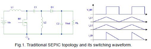
Formula (1) shows its input and output steady state relationship, which is a buck/boost type.

However, it is none isolation type, it will be limited in some applications, so we need to transform it into an isolation type.
Here we show the transform process, we suppose that we can replace the inductor L2 with an ideal coupled transformer T1, just like Fig.2 showed, the circuit still can work well.
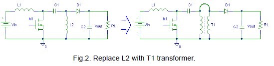
For ideal transformer’s couple coefficient is 1, so that the voltage between two transformer terminals is zero, there will be no current follow through the wire connected between two terminals, so we can cut the wire without affect the converter working. After that, we get a final transformed isolate type SEPIC topology as showed in Fig.3, and also its switching waveform showed in Fig.4.

3. Theory analyze and simulation
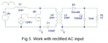
Carefully examine the circuit of Fig.3, there is an inductor at input, and it can work as a PFC choke, and L1 and M1 form a circuit which is similar to boost converter, so we can utilize it as a PFC correction stage. And T1 C1 and M1 form a fly back converter to transfer power to secondary side.
As Fig.5 shown, we change the circuits input to AC rectified input, and use the parameters as figure shown, and apply a 50kHz 5uS fixed on time control signal to drive the Mosfet.
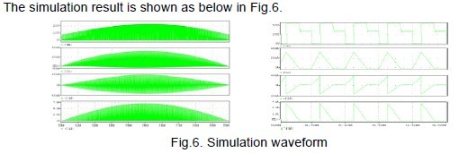
From the waveform, we can find that L1 peak current is varied as sinusoid. If we use fixed on time’s boundary conduction driving mode to drive the Mosfet, then L1 current waveform will look like this type, and its average current is also sinusoidal, just like Fig.7 showed, then PFC function can be achieved.
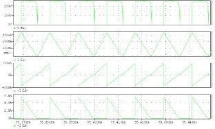
Fig.7. Waveform of driving by fixed on time boundary conduction mode In traditional fly back type single stage circuit, input current is discontinuous when 85
Mosfet is turned off, though input peak current is sinusoid, but the average input current is not sinusoid, so the THD will be poor.
Compared with old topology, this new circuit’s input current is continuous whenever Mosfet is on or off, so it would have better THD than original method, and for its input current is continuous, it will be easier for input stage’s low pass filter design to pass EMC.
4. CC/CV mechanism
In order to guarantee working at boundary conduction mode, and also achieve primary regulation, an auxiliary winding is needed to detect secondary side voltage and zero current point.
Fig.8 shows a rough circuit to realize those functions.
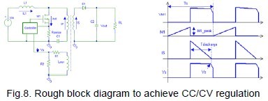
Controller acquires the secondary side voltage by sampling the Vs voltage which is divided from the well coupled auxiliary winding, and also detect the secondary side conduction time Tdischarge.
Then:

From formula (2), we find that Vs is proportional to the Vout, and we can use Vs as feed back input to control driving duty to achieve CV regulation without second side feed back, output voltage can be changed by adjust the ratio of divider R1/R2.
And then:

From the formula (3), the secondary output current Iout is proportional to the value of use this value as the input of CC regulation feed back to control the converter output duty, then CC regulation function can be achieved too, secondary output constant current point can be set by adjust the value of sensing resistor Rsense.
5. Feed back parameter design
When work with the AC rectified input, the converter is working at boundary conduction mode under fixed on time modulation mechanism, so the input and output average current are sinusoidal.
Sinusoidal input current gets high PF. but sinusoid output current causes big ripple of load current, especially with such kind of LED load, which’s characteristic seems more like a CV load. So if the requirement for ripple current is lower, bigger output capacitor is needed to filter the 100/120Hz ripple current.
In order to achieve fixed on time modulation and get better PF, the CC close loop band width must be as lower as 6~10Hz. Low band width will cause output current big overshoot, it will cause LED lamp blinking during turn on, so adding a soft start or overshoot eliminator is essential.
6. Waveform and test result
Till now, we have introduced the new topology of isolation type single stage converter, it requires for fixed on time’s boundary conduction mode driving to achieve high PF and easy way to realize PSR function.
However, we also can use fixed frequency type PSR controller to drive this converter, we insert a block diode D2 to prevent L1 current reverse and D3 as a damper to clamp stray resonation between D2 and L1. And to decrease secondary side ripple current, we use bigger C1 as bulk capacitor to smooth the energy transferred to second side.Fig 9 shows the modification.
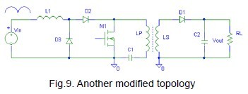
The advantage of the modification is you can realize both PFC and PSR regulation with normal PSR controller, the disadvantage is the THD is worsen due to fixed frequency driving.
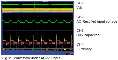
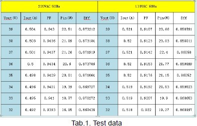
Fig.10 and 11 show the test waveform got from 20V0.5A LED lamp power which using this topology, and also the test result in Tab.1.

7. Conclusion
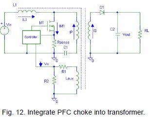
From the description above, this topology can be a good choice for the LED application which require for both high PF and PSR function. The disadvantage is that it needs an extra inductor as PFC choke. It limits its application in some small power application which has critical size limitation. Further research will try to integrate this inductor into transformer for more compact size, and loose coupled to main transformer to minimize the input current switching ripple, such as Fig.12 shows.
Reference
[1]. Fairchild, AN-6067, Design and Application of Primary-Side Regulation (PSR)PWM Controller.
[2]. Fairchild, AN-8033, Design Guideline for Primary Side Regulated (PSR) Flyback Converter Using FAN103 and FSEZ13X7.
Biography
Stephen Li is graduated from Huazhong Science and Technology University in 1995,and has many years of experience in RD department before join Fairchild. Now he is working at Fairchild Xiamen office and major takes charge of display and lighting customer application support.